ZHCSFN3E August   2006  – January 2021 INA193A-Q1 , INA194A-Q1 , INA195A-Q1 , INA196A-Q1 , INA197A-Q1 , INA198A-Q1

PRODUCTION DATA  

  1. 特性
  2. 应用
  3. 说明
  4. Revision History
  5. Pin Configuration and Functions
  6. Specifications
    1. 6.1 Absolute Maximum Ratings
    2. 6.2 ESD Ratings
    3. 6.3 Recommended Operating Conditions
    4. 6.4 Thermal Information
    5. 6.5 Electrical Characteristics
    6. 6.6 Typical Characteristics
  7. Detailed Description
    1. 7.1 Overview
    2. 7.2 Functional Block Diagram
    3. 7.3 Feature Description
      1. 7.3.1 Basic Connection
      2. 7.3.2 Selecting RS
      3. 7.3.3 Inside the INA19xA
      4. 7.3.4 Power Supply
    4. 7.4 Device Functional Modes
      1. 7.4.1 Input Filtering
      2. 7.4.2 Accuracy Variations as a Result Of VSENSE and Common Mode Voltage
        1. 7.4.2.1 Normal Case 1: VSENSE ≥ 20 mV, VCM ≥ VS
        2. 7.4.2.2 Normal Case 2: VSENSE ≥ 20 mV, VCM < VS
        3. 7.4.2.3 Low VSENSE Case 1: VSENSE < 20 mV, –16 V ≤ VCM < 0; and Low VSENSE Case 3: VSENSE < 20 mV, VS < VCM ≤ 80 V
        4. 7.4.2.4 Low VSENSE Case 2: VSENSE < 20 mV, 0 V ≤ VCM ≤ VS
      3. 7.4.3 Shutdown
      4. 7.4.4 Transient Protection
      5. 7.4.5 Output Voltage Range
  8. Application and Implementation
    1. 8.1 Application Information
    2. 8.2 Typical Application
      1. 8.2.1 Design Requirements
      2. 8.2.2 Detailed Design Procedure
      3. 8.2.3 Application Curve
  9. Power Supply Recommendations
  10. 10Layout
    1. 10.1 Layout Guidelines
      1. 10.1.1 RFI/EMI
    2. 10.2 Layout Example
  11. 11Device and Documentation Support
    1. 11.1 接收文档更新通知
    2. 11.2 支持资源
    3. 11.3 Trademarks
    4. 11.4 静电放电警告
    5. 11.5 术语表
  12. 12Mechanical, Packaging, and Orderable Information

封装选项

机械数据 (封装 | 引脚)
散热焊盘机械数据 (封装 | 引脚)
订购信息

Low VSENSE Case 2: VSENSE < 20 mV, 0 V ≤ VCM ≤ VS

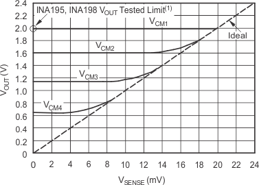
This region of operation is the least accurate for the INA19xA-Q1 family. To achieve the wide input common mode voltage range, these devices use two operational amplifier front ends in parallel. One operational amplifier front end operates in the positive input common mode voltage range, and the other in the negative input region. For this case, neither of these two internal amplifiers dominates and overall loop gain is very low. Within this region, VOUT approaches voltages close to linear operation levels for Normal Case 2. This deviation from linear operation becomes greatest the closer VSENSE approaches 0 V. Within this region, as VSENSE approaches 20 mV, device operation is closer to that described by Normal Case 2. Figure 7-8 illustrates this behavior for the INA195A. The VOUT maximum peak for this case is tested by maintaining a constant VS, setting VSENSE = 0 mV and sweeping VCM from 0 V to VS. The exact VCM at which VOUT peaks during this test varies from part to part, but the VOUT maximum peak is tested to be less than the specified VOUT tested limit.
GUID-E1CD1F9D-0B28-4A99-8D01-F4171A35EDB3-low.gif
INA193, INA196 VOUT Tested Limit = 0.4 V
INA194, INA197 VOUT Tested Limit = 1 V
VOUT tested limit at VSENSE = 0 mV, 0 ≤ VCM1 ≤ VS.
VCM2, VCM3, and VCM4 illustrate the variance from part to part of the VCM that can cause maximum VOUT with VSENSE < 20 mV.
Figure 7-8 Example for Low VSENSE Case 2 (INA195A, INA198A: Gain = 100)