ZHCS170C April 2011 – April 2016 INA200-Q1 , INA201-Q1 , INA202-Q1
PRODUCTION DATA.
- 1 特性
- 2 应用
- 3 说明
- 4 修订历史记录
- 5 Device Comparison Table
- 6 Pin Configuration and Functions
- 7 Specifications
- 8 Parameter Measurement Information
- 9 Detailed Description
- 10Application Information
- 11Power Supply Recommendations
- 12Layout
- 13器件和文档支持
- 14机械、封装和可订购信息
10 Application Information
NOTE
Information in the following applications sections is not part of the TI component specification, and TI does not warrant its accuracy or completeness. TI’s customers are responsible for determining suitability of components for their purposes. Customers should validate and test their design implementation to confirm system functionality.
10.1 Application Information
The INA20x-Q1 series is designed to enable easy configuration for detecting overcurrent conditions and current monitoring in an application. This device is individually targeted towards overcurrent detection of a single threshold. However, this device can also be paired with additional devices and circuitry to create more complex monitoring functional blocks.
10.1.1 Basic Connections
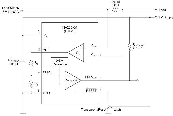
Figure 27 shows the basic connections of the INA200-Q1, INA201-Q1, and INA202-Q1. Connect the input pins, VIN+ and VIN–, as close as possible to the shunt resistor to minimize any resistance in series with the shunt resistance.
Stability requires the use of power-supply bypass capacitors. Applications with noisy or high-impedance power supplies may require additional decoupling capacitors to reject power-supply noise. Connect bypass capacitors close to the device pins.
 Figure 27. INA200-Q1 Basic Connections
10.1.2 Selecting RS
The value chosen for the shunt resistor, RS, depends on the application and is a compromise between small-signal accuracy and maximum permissible voltage loss in the measurement line. High values of RS provide better accuracy at lower currents by minimizing the effects of offset, whereas low values of RS minimize voltage loss in the supply line. Most applications attain best performance with an RS value that provides a full-scale shunt voltage range of 50 mV to 100 mV. Maximum input voltage for accurate measurements is 500 mV, but output voltage is limited by supply.
10.1.3 Input Filtering
An obvious and straightforward location for filtering is at the output of the INA20x-Q1 series; however, this location negates the advantage of the low output impedance of the internal buffer. The only other option for filtering is at the input pins of the INA20x-Q1, but the internal 5-kΩ + 30% input impedance complicates input filtering, as illustrated in Figure 28. Use the lowest possible resistor values to minimize both the initial shift in gain and effects of tolerance. Equation 1 gives the effect on initial gain:

To calculate the total effect on gain error, replace the 5-kΩ term with 5 kΩ – 30%, (or 3.5 kΩ) or 5 kΩ + 30% (or 6.5 kΩ). One can also be insert the tolerance extremes of RFILT into the equation. If using a pair of 100-Ω 1% resistors on the inputs, the initial gain error is 1.96%. Worst-case tolerance conditions always occur at the lower excursion of the internal 5-kΩ resistor (3.5-kΩ), and the higher excursion of RFILT + 3% in this case.
Note that one must then combine the specified accuracy of the INA20x-Q1 in addition to these tolerances. Although this discussion treated worst-case accuracy conditions by combining the extremes of the resistor values, it is appropriate to use geometric-mean or root-sum-square calculations to total the effects of accuracy variations.
10.1.4 Accuracy Variations as a Result of VSENSE and Common-Mode Voltage
The accuracy of the INA20x-Q1 current-shunt monitors is a function of two main variables: VSENSE (VIN+ – VIN–) and common-mode voltage, VCM, relative to the supply voltage, VS. The expression for VCM is (VIN+ + VIN–) / 2; however, in practice, VCM is effectively the voltage at VIN+ because the voltage drop across VSENSE is usually small.
This section addresses the accuracy of these specific operating regions:
- Normal Case 1: VSENSE ≥ 20 mV, VCM ≥ VS
- Normal Case 2: VSENSE ≥ 20 mV, VCM < VS
- Low VSENSE Case 1: VSENSE < 20 mV, –16 V ≤ VCM < 0
- Low VSENSE Case 2: VSENSE < 20 mV, 0V ≤ VCM ≤ VS
- Low VSENSE Case 3: VSENSE < 20 mV, VS < VCM ≤ 80 V
10.1.4.1 Normal Case 1: VSENSE ≥ 20 mV, VCM ≥ VS
This region of operation provides the highest accuracy. Here, use of a two-step method characterizes and measures the input offset voltage. First, Equation 2 determines the gain.

where:
VOUT1 = output voltage with VSENSE = 100 mV
VOUT2 = output voltage with VSENSE = 20 mV
Then the offset voltage is measured at VSENSE = 100 mV and referred to the input (RTI) of the current shunt monitor, as shown in Equation 3.

In the Typical Characteristics, Figure 6 (Output Error versus Common-Mode Voltage curve) shows the highest accuracy for the this region of operation. In this plot, VS = 12 V; for VCM ≥ 12 V, the output error is at its minimum. Using this case also creates the VSENSE ≥ 20 mV output specifications in the Electrical Characteristics: Current-Shunt Monitor table.
10.1.4.2 Normal Case 2: VSENSE ≥ 20 mV, VCM < VS
This region of operation has slightly less accuracy than Normal Case 1 as a result of the common-mode operating area in which the part functions, as seen in the Figure 6 (Output Error versus Common-Mode Voltage curve). As noted, for this graph VS = 12 V; for VCM < 12 V, the output error increases as VCM becomes less than 12 V, with a typical maximum error of 0.005% at the most negative VCM = –16 V.
10.1.4.3 Low VSENSE Case 1: VSENSE < 20 mV, –16 V ≤ VCM < 0 V; and
Low VSENSE Case 3: VSENSE < 20 mV, VS < VCM ≤ 80 V
Although not designed for accurate operation in either of these regions, the INA20x-Q1 family of devices may have exposure to these conditions in some applications. For example, when monitoring power supplies being switched on and off with VS still applied to the INA20x-Q1, it is important to know what the device behavior is in these regions.
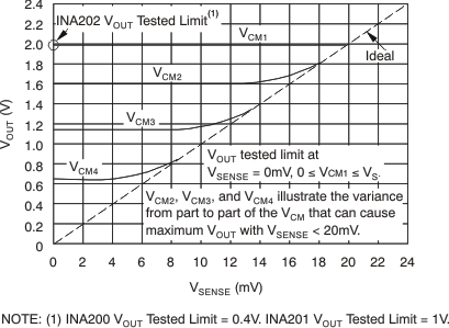
As VSENSE approaches 0 mV, in these VCM regions, the device output accuracy degrades. A larger-than-normal offset can appear at the current shunt monitor output with a typical maximum value of VOUT = 300 mV for VSENSE = 0 mV. As VSENSE approaches 20 mV, VOUT returns to the expected output value with accuracy, as specified in the Electrical Characteristics: Current-Shunt Monitor. Figure 29 illustrates this effect using the INA202-Q1 (gain = 100).
 Figure 29. Example for Low VSENSE Cases 1 and 3 (INA202-Q1, Gain = 100)
10.1.4.4 Low VSENSE Case 2: VSENSE < 20 mV, 0 V ≤ VCM ≤ VS
This region of operation is the least accurate for the INA20x-Q1 family. To achieve the wide input common-mode voltage range, these devices use two op amp front ends in parallel. One op amp front end operates in the positive-input common-mode voltage range, and the other in the negative-input region. For this case, neither of these two internal amplifiers dominates, and overall loop gain is very low. Within this region, VOUT approaches voltages close to linear operation levels for normal case 2. This deviation from linear operation becomes greatest the closer VSENSE approaches 0 V. Within this region, as VSENSE approaches 20 mV, device operation is closer to that described by normal case 2. Figure 30 illustrates this behavior for the INA202-Q1. To test the VOUT maximum peak for this case, maintain a constant VS, set VSENSE = 0 mV, and sweep VCM from 0 V to VS. The exact VCM at which VOUT peaks during this test varies from part to part, but the tested VOUT maximum peak for any part is less than the specified VOUT test limit.
 Figure 30. Example for Low VSENSE Case 2 (INA202-Q1, Gain = 100)
10.1.5 Transient Protection
The –16-V to +80-V common-mode range of the INA20X-Q1 is ideal for withstanding automotive fault conditions, ranging from 12-V battery reversal up to 80-V transients, because there is need for additional protective components up to those levels. In the event that the INA20x-Q1 are exposed to transients on the inputs in excess of their ratings, then external transient absorption with semiconductor transient absorbers (such as Zeners) is necessary. Do not use metal-oxide varistors (MOVs) or voltage-dependent resistors (VDRs) except when they are used in addition to a semiconductor transient absorber. Select the transient absorber such that it never allows exposure of the INA20X-Q1 to transients greater than 80 V (that is, allow for transient absorber tolerance, as well as additional voltage due to transient absorber dynamic impedance). Despite the use of internal zener-type ESD protection, the INA20x-Q1 do not lend themselves to using external resistors in series with the inputs, because the internal gain resistors can vary up to ±30%. (If gain accuracy is not important, then one can add resistors in series with the INA20x-Q1 inputs with two equal resistors on each input.)
10.2 Typical Applications
10.2.1 Low-Side Switch Overcurrent Shutdown
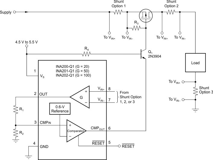
The INA20x-Q1 measures current through a resistive shunt with current flowing in one direction, thus enabling detection of an overcurrent event only when the differential input voltage exceeds the threshold limit. When the current reaches the set limit of the divider R1 / R2, the output of CMPOUT transitions high and Q1 turns on and pull the gate of the Pass-FET low and turn off the flow off current.

10.2.1.1 Design Requirements
For this design example, use the input parameters shown in Table 1. All other register settings are default.
Table 1. Design Parameters
| DESIGN PARAMETER | EXAMPLE VALUE |
|---|---|
| Supply voltage, VS | 3.3 V |
| R2 / R1 | 1.5 |
| R2 | 15 kΩ |
| R1 | 10 kΩ |
| Gain | 20 V/V (INA200-Q1) |
| Shunt resistor, RSHUNT | 5 mΩ |
| Desired trip current, ITRIP | 1 A |
10.2.1.2 Detailed Design Procedure
Figure 31 shows the basic connections for a low-side, switch overcurrent shutdown application. Connect input pins IN+ and IN– as close as possible to the current-sensing resistor (RSHUNT) to minimize any resistance in series with the shunt resistance. Additional resistance between the current-sensing resistor and input pins can result in errors in the measurement. When input current flows through this external input resistance, the voltage developed across the shunt resistor can differ from the voltage reaching the input pins. Connect the input pins to one of the three shunt options shown in Figure 31.
Use the device gain and shunt resistor value to calculate the OUT pin voltage, VOUT_TRIP, for the desired trip current, as shown in Equation 4:
where
- ITRIP = Desired trip current
- RSHUNT = Shunt resistor value
Configure R1 and R2 so that the current trip point is equal to the 0.6-V reference voltage, as shown in Equation 5:
10.2.1.3 Application Curves
 Figure 32. Low-Side Switch Overcurrent Shutdown Response
10.2.2 High-Side Switch Overcurrent Shutdown
Figure 33 shows the basic connection for a high-side, switch overcurrent shutdown application. The high-side PMOS switch disconnects when an overcurrent event occurs. The previous Detailed Design Procedure section describes how to apply this application example. The difference is that the current is sensed on the high side of the bus in this application, and the low side of the bus in the previous application example.

10.2.3 Bidirectional Overcurrent Comparator
Figure 34 shows the basic connection for a bidirectional overcurrent comparator using two INA20x-Q1 devices of the same gain.

