ZHCSFN4E November 2006 – September 2017 INA200 , INA201 , INA202
PRODUCTION DATA.
- 1 特性
- 2 应用
- 3 说明
- 4 修订历史记录
- 5 Pin Configuration and Functions
- 6 Specifications
- 7 Detailed Description
- 8 Application and Implementation
- 9 Power Supply Recommendations
- 10Layout
- 11器件和文档支持
- 12机械、封装和可订购信息
7 Detailed Description
7.1 Overview
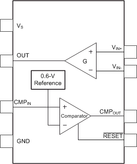
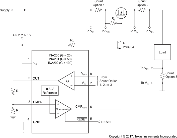
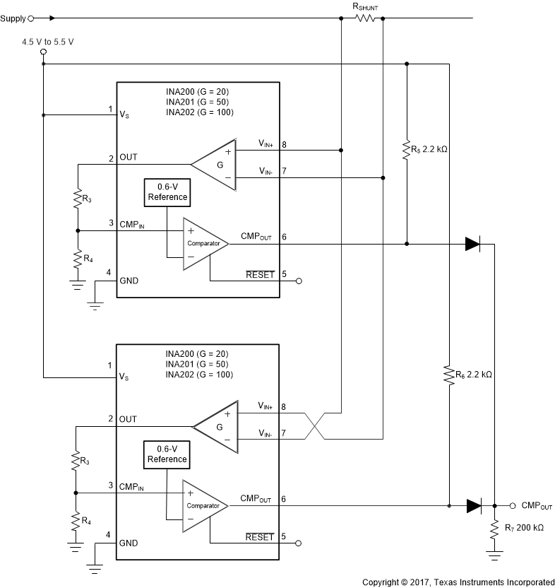
The INA200, INA201, and INA202 devices are high-side current-shunt monitors with voltage output. The INA20x devices can sense drops across shunts at common-mode voltages from –16 V to 80 V. The INA200–INA202 devices are available with three output voltage scales: 20 V/V, 50 V/V, and 100 V/V, with up to 500-kHz bandwidth. The INA200, INA201, and INA202 devices incorporate an open-drain comparator and internal reference providing a 0.6-V threshold. External dividers set the current trip point. The comparator includes a latching capability, that can be made transparent by grounding (or leaving open) the RESET pin. The INA200, INA201, and INA202 devices operate from a single 2.7 to 18-V supply, drawing a maximum of 1800 μA of supply current. Package options include the very small MSOP-8 and the SO-8. All versions are specified over the extended operating temperature range of –40°C to +125°C.
7.2 Functional Block Diagram
7.3 Feature Description
7.3.1 Basic Connections
Figure 26 shows the basic connections of the INA20x devices. The input pins (VIN+ and VIN–) must be connected as closely as possible with Kelvin connections to the shunt resistor to minimize any resistance in series with the shunt resistance.
Power-supply bypass capacitors are required for stability. Applications with noisy or high-impedance power supplies may require additional decoupling capacitors to reject power-supply noise. Connect bypass capacitors close to the device pins.
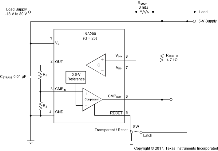 Figure 26. INA200 Basic Connections
7.3.2 Selecting RS
The selected value for the shunt resistor, RS, depends on the application and is a compromise between small-signal accuracy and maximum permissible voltage loss in the measurement line. High values of RS provide better accuracy at lower currents by minimizing the effects of offset, while low values of RS minimize voltage loss in the supply line. For most applications, using an RS value that provides a full-scale shunt voltage range of 50 mV to 100 mV results in the best performance. Maximum input voltage for accurate measurements is 500 mV, but output voltage is limited by supply.
7.3.3 Comparator
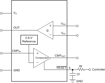
The INA200, INA201, and INA202 devices incorporate an open-drain comparator. This comparator typically has 2 mV of offset and a 1.3-μs (typical) response time. The output of the comparator latches and is reset through the RESET pin; see Figure 28.
When Vs and RESET are different, TI recommends adding a low-pass filter (LPF) on the RESET pin to avoid comparator behavior inconsistent with the data sheet. For instance, with a 12-V supply and a 3.3-V RESET, a rise time of 400 ns is appropriate. Similarly, with an 18-V supply and a 2.7-V RESET, a 1-µs rise time is appropriate; see Figure 31.
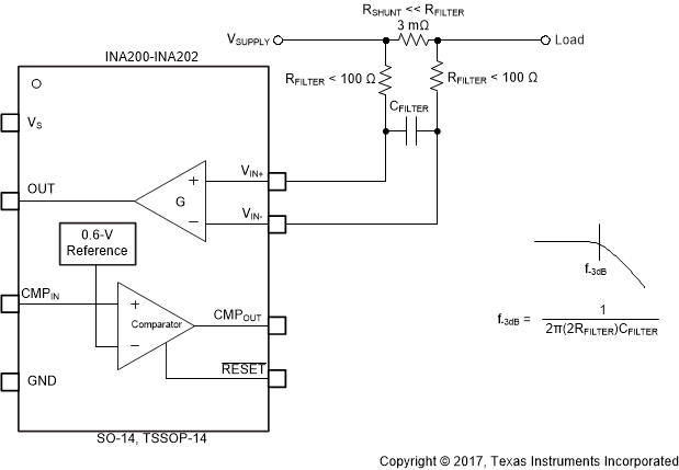 Figure 27. Input Filter (Gain Error: 1.5% to 2.8%)
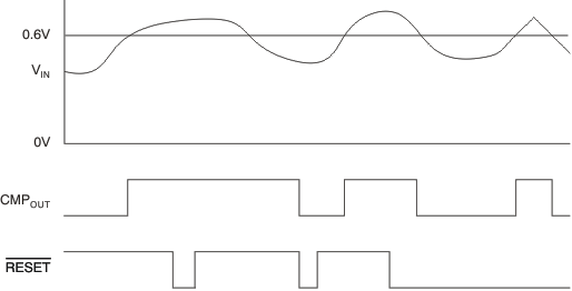 Figure 28. Comparator Latching Capability
7.4 Device Functional Modes
7.4.1 Input Filtering
An obvious and straightforward location for filtering is at the output of the INA20x series; however, this location negates the advantage of the low output impedance of the internal buffer. The only other option for filtering is at the input pins of the INA20x devices, which is complicated by the internal 5 kΩ + 30% input impedance. This is shown in Figure 27. Using the lowest possible resistor values minimizes the initial shift in gain and effects of tolerance. The effect on initial gain is shown in Equation 1:

Total effect on gain error can be calculated by replacing the 5-kΩ term with 5 kΩ – 30%, (or 3.5 kΩ) or 5 kΩ + 30% (or 6.5 kΩ). The tolerance extremes of RFILT can be inserted into the equation. If a pair of 100-Ω 1% resistors are used on the inputs, the initial gain error equals 1.96%. Worst-case tolerance conditions always occur at the lower excursion of the internal 5-kΩ resistor (3.5 kΩ), and the higher excursion of RFILT – 3% in this case.
The specified accuracy of the INA20x devices must then be combined in addition to these tolerances. While this discussion treated accuracy worst-case conditions by combining the extremes of the resistor values, it is appropriate to use geometric mean or root sum square calculations to total the effects of accuracy variations.
7.4.2 Accuracy Variations as a Result of VSENSE and Common-Mode Voltage
The accuracy of the INA200, INA201, and INA202 current shunt monitors is a function of two main variables: VSENSE (VIN+ – VIN–), common-mode voltage, (VCM), relative to the supply voltage (VS). VCM is expressed as (VIN+ + VIN–) / 2; however, in practice, VCM is seen as the voltage at VIN+ because the voltage drop across VSENSE is typically small.
This section addresses the accuracy of these specific operating regions:
- Normal Case 1: VSENSE ≥ 20 mV, VCM ≥ VS
- Normal Case 2: VSENSE ≥ 20 mV, VCM < VS
- Low VSENSE Case 1: VSENSE < 20 mV, –16 V ≤ VCM < 0
- Low VSENSE Case 2: VSENSE < 20 mV, 0 V ≤ VCM ≤ VS
- Low VSENSE Case 3: VSENSE < 20 mV, VS < VCM ≤ 80 V
7.4.2.1 Normal Case 1: VSENSE ≥ 20 mv, VCM ≥ VS
This region of operation provides the highest accuracy. Here, the input offset voltage is characterized and measured using a two-step method. First, the gain is determined by Equation 2.

where
- VOUT1 = output voltage with VSENSE = 100 mV
- VOUT2 = output voltage with VSENSE = 20 mV
Then the offset voltage is measured at VSENSE = 100 mV, and referred to the input (RTI) of the current shunt monitor, as shown in Electrical Characteristics: Current-Shunt Monitor.

In the Typical Characteristics, Figure 7 shows the highest accuracy for the this region of operation. In this plot, VS = 12 V. For VCM ≥ 12 V, the output error is at the minimum value. This case creates the VSENSE ≥ 20-mV output specifications in Electrical Characteristics: Current-Shunt Monitor .
7.4.2.2 Normal Case 2: VSENSE ≥ 20 mv, VCM < VS
This region of operation is less accurate than normal case 1 as a result of the common-mode operating area in which the part functions, as shown in the Figure 7 curve (Figure 7). As noted, for this graph VS = 12 V; for VCM < 12 V, the output error increases as VCM decreases to less than 12 V, with a typical maximum error of 0.005% at the most negative VCM = –16 V.
7.4.2.3 Low VSENSE Case 1: VSENSE < 20 mV, –16 V ≤ VCM < 0
and Low VSENSE Case 3: VSENSE < 20 mV, VS < VCM ≤ 80 V
Although the INA200 family of devices are not designed for accurate operation in these regions, some applications are exposed to these conditions. For example, when monitoring power supplies that are switched on and off while VS is still applied to the INA20x devices, it is important to know what the behavior of the devices is in these regions.
As VSENSE approaches 0 mV, in these VCM regions, the accuracy of the device output degrades. A larger-than-normal offset can appear at the current shunt monitor output with a typical maximum value of VOUT = 300 mV for
VSENSE = 0 mV. As VSENSE approaches 20 mV, VOUT returns to the expected output value with accuracy as shown in Electrical Characteristics: Current-Shunt Monitor. Figure 32 shows this effect using the INA202 (gain = 100).
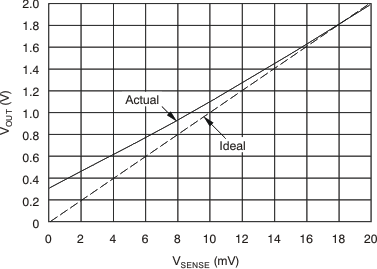 Figure 32. Example For Low VSENSE Cases 1 and 3 (INA202, Gain = 100)
7.4.2.4 Low VSENSE Case 2: VSENSE < 20 mV, 0 V ≤ VCM ≤ VS
This region of operation is the least accurate for the INA20x family. To achieve the wide input common-mode voltage range, these devices use two op amp front ends in parallel. One op amp front end operates in the positive input common-mode voltage range, and the other in the negative input region. For this case, neither of these two internal amplifiers dominates and overall loop gain is low. Within this region, VOUT approaches voltages close to linear operation levels for normal case 2. This deviation from linear operation becomes greatest the closer VSENSE approaches 0 V. Within this region, as VSENSE approaches 20 mV, device operation is closer to that is described in normal case 2. Figure 33 shows this behavior for the INA202. The VOUT maximum peak for this case is tested by maintaining a constant VS, setting VSENSE equal to 0 mV and sweeping VCM from 0 V to VS. The exact VCM at which VOUT peaks during this test varies from device to device, but the VOUT maximum peak is tested to be less than the specified VOUT tested limit.
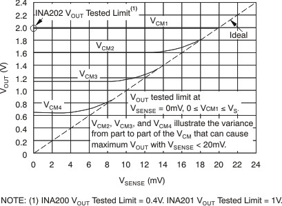 Figure 33. Example For Low VSENSE Case 2 (INA202, Gain = 100)
7.4.3 Transient Protection
The –16 to 80 V common-mode range of the INA20x devices is ideal for withstanding automotive fault conditions ranging from 12-V battery reversal up to 80-V transients, since no additional protective components are required up to those levels. In the event that the INA20x devices are exposed to transients on the inputs in excess of their ratings, then external transient absorption with semiconductor transient absorbers (such as Zeners) are required. TI does not recommend using MOVs or VDRs, except when they are used in addition to a semiconductor transient absorber. Select the transient absorber so the absorber does not allow the INA20x devices to be exposed to transients greater than 80 V (that is, allow for transient absorber tolerance and additional voltage due to transient absorber dynamic impedance). Despite the use of internal Zener-type ESD protection, the INA20x devices do not lend themselves to using external resistors in series with the inputs since the internal gain resistors can vary up to ±30%. (If gain accuracy is not important, then resistors can be added in series with the INA200, INA201, and INA202 inputs with two equal resistors on each input.)
7.4.4 Output Voltage Range
The output of the INA20x devices is accurate within the output voltage swing range set by the power supply pin (VS.) This performance is best illustrated when using the INA202 (a gain of 100 version), where a 100-mV full-scale input from the shunt resistor requires an output voltage swing of 10 V, and a power-supply voltage sufficient to achieve 10 V on the output.
