ZHCSFN6F March 2007 – June 2021 INA203 , INA204 , INA205
PRODUCTION DATA
- 1 特性
- 2 应用
- 3 说明
- 4 Revision History
- 5 Pin Configuration and Functions
-
6 Specifications
- 6.1 Absolute Maximum Ratings
- 6.2 ESD Ratings
- 6.3 Recommended Operating Conditions
- 6.4 Thermal Information
- 6.5 Electrical Characteristics: Current-Shunt Monitor
- 6.6 Electrical Characteristics: Comparator
- 6.7 Electrical Characteristics: Reference
- 6.8 Electrical Characteristics: General
- 6.9 Typical Characteristics
- 7 Detailed Description
- 8 Application and Implementation
- 9 Power Supply Recommendations
- 10Layout
- 11Device and Documentation Support
- 12Mechanical, Packaging, and Orderable Information
封装选项
请参考 PDF 数据表获取器件具体的封装图。
机械数据 (封装 | 引脚)
- D|14
- DGS|10
- PW|14
散热焊盘机械数据 (封装 | 引脚)
订购信息
7.4.2.3 Low VSENSE Case 1
- VSENSE < 20 mV, –16 V ≤ VCM< 0;
- Low VSENSE Case 3:
- VSENSE < 20 mV, VS < VCM ≤ 80 V
Although the INA203 family of devices are not designed for accurate operation in either of these regions, some applications are exposed to these conditions; for example, when monitoring power supplies that are switched on and off while VS is still applied to the INA203, INA204, or INA205. Take care to know what the behavior of the devices will be in these regions.
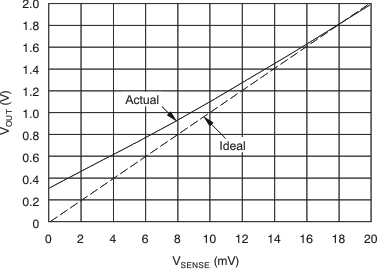
As VSENSE approaches 0 mV, in these VCM regions, the device output accuracy degrades. A larger-than-normal offset can appear at the current shunt monitor output with a typical maximum value of VOUT = 300 mV for VSENSE = 0 mV. As VSENSE approaches 20 mV, VOUT returns to the expected output value with accuracy as specified in the Section 6.5. Figure 7-11 illustrates this effect using the INA205 (Gain = 100).
 Figure 7-11 Example for Low VSENSE Cases 1 and 3 (INA205, Gain = 100)