ZHCSFN6F March 2007 – June 2021 INA203 , INA204 , INA205
PRODUCTION DATA
- 1 特性
- 2 应用
- 3 说明
- 4 Revision History
- 5 Pin Configuration and Functions
-
6 Specifications
- 6.1 Absolute Maximum Ratings
- 6.2 ESD Ratings
- 6.3 Recommended Operating Conditions
- 6.4 Thermal Information
- 6.5 Electrical Characteristics: Current-Shunt Monitor
- 6.6 Electrical Characteristics: Comparator
- 6.7 Electrical Characteristics: Reference
- 6.8 Electrical Characteristics: General
- 6.9 Typical Characteristics
- 7 Detailed Description
- 8 Application and Implementation
- 9 Power Supply Recommendations
- 10Layout
- 11Device and Documentation Support
- 12Mechanical, Packaging, and Orderable Information
封装选项
请参考 PDF 数据表获取器件具体的封装图。
机械数据 (封装 | 引脚)
- D|14
- DGS|10
- PW|14
散热焊盘机械数据 (封装 | 引脚)
订购信息
7.3.5 Comparator Maximum Input Voltage Range
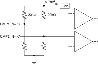
The maximum voltage at the comparator input for normal operation is up to (Vs) – 1.5 V. There are special considerations when overdriving the reference inputs (pins 3 and 6). Driving either or both inputs high enough to drive 1 mA back into the reference introduces errors into the reference. Figure 7-6 shows the basic input structure. A general guideline is to limit the voltage on both inputs to a total of 20 V. The exact limit depends on the available voltage and whether either or both inputs are subject to the large voltage. When making this determination, consider the 20 kΩ from each input back to the comparator. Figure 7-7 shows the maximum input voltage that avoids creating a reference error when driving both inputs (an equivalent resistance back into the reference of 10 kΩ).
 Figure 7-6 Limit Current Into Reference ≤ 1 mA
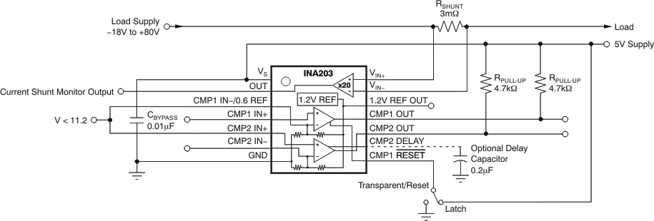
 Figure 7-7 Overdriving Comparator Inputs Without Generating a Reference Error
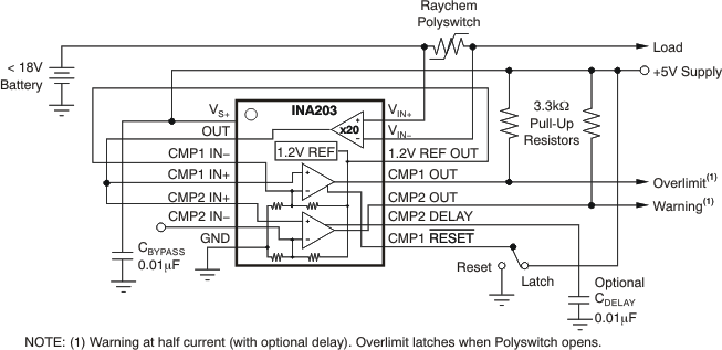
 Figure 7-8 Polyswitch Warning and Fault Detection Circuit
 Figure 7-9 Lead-Acid Battery Protection Circuit