ZHCSO32C September 2000 – January 2022 INA126 , INA2126
PRODUCTION DATA
- 1 特性
- 2 应用
- 3 说明
- 4 Revision History
- 5 Pin Configuration and Functions
- 6 Specifications
- 7 Detailed Description
- 8 Application and Implementation
- 9 Power Supply Recommendations
- 10Layout
- 11Device and Documentation Support
- 12Mechanical, Packaging, and Orderable Information
8.2 Typical Application
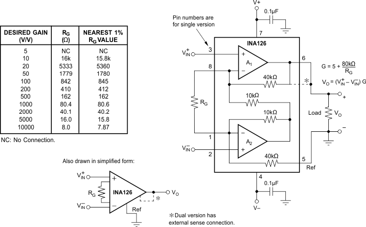
Figure 8-1 shows the basic connections required for operation of the INA126. Applications with noisy or high impedance power supplies may require decoupling capacitors close to the device pins as shown.
The output is referred to the output reference (Ref) pin, which is normally grounded. This connection must be low-impedance to maintain good common-mode rejection. A resistance of 8 Ω in series with the Ref pin causes a typical device to degrade to approximately 80-dB CMR.
Figure 8-4 depicts a desired differential signal from a sensor at 1 kHz and 5 mVPP superimposed on top of a 1-VPP, 60-Hz common-mode signal (the 1-kHz signal can not be resolved in this scope trace). The FFT trace in Figure 8-5 shows the two signals. Figure 8-6 shows the clearly recovered differential signal at the output of the INA126 operating at a gain of 250. The FFT of Figure 8-7 shows the 60-Hz common-mode is no longer visible.
The dual version INA2126 has feedback-sense connections, SenseA and SenseB, that must be connected to the respective output pins for proper operation. The sense connection can sense the output voltage directly at the load for best accuracy.
 Figure 8-1 Basic Connections