ZHCSRV7B december 1995 – may 2023 INA2128
PRODUCTION DATA
7.2.9 Channel Crosstalk
The two channels of the INA2128 are completely independent, including all bias circuitry. At dc and low frequency, there is virtually no signal coupling between channels. Crosstalk increases with frequency and depends on circuit gain, source impedance, and signal characteristics.
As source impedance increases, careful circuit layout helps achieve lowest channel crosstalk. Most crossstalk is produced by capacitive coupling of signals from one channel to the input section of the other channel. To minimize coupling, separate the input traces as far as practical from any signals associated with the opposite channel. A grounded guard trace surrounding the inputs helps reduce stray coupling between channels. Run the differential inputs of each channel parallel to each other or directly adjacent on top and bottom side of a circuit board. Stray coupling then tends to produce a common-mode signal which is rejected by the IA input.
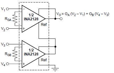
 Figure 7-5 Sum of Differences Amplifier
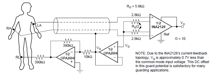
 Figure 7-6 ECG Amplifier With Right-Leg
Drive