ZHCSRV7B december 1995 – may 2023 INA2128
PRODUCTION DATA
7.2.6 Input Common-Mode Range
The linear input voltage range of the input circuitry of the INA2128 is from approximately 1.4 V less than the positive supply voltage to 1.7 V greater than the negative supply. As a differential input voltage causes the output voltage increase, the linear input range is limited by the output voltage swing of amplifiers A1 and A2. Therefore, the linear common-mode input range is related to the output voltage of the complete amplifier. This behavior also depends on supply voltage—see performance curves Figure 6-6 and Figure 6-5.
Input-overload can produce an output voltage that appears normal. For example, if an input overload condition drives both input amplifiers to the positive output swing limit, the difference voltage measured by the output amplifier is near zero. The output of the INA2128 is near 0 V even though both inputs are overloaded.
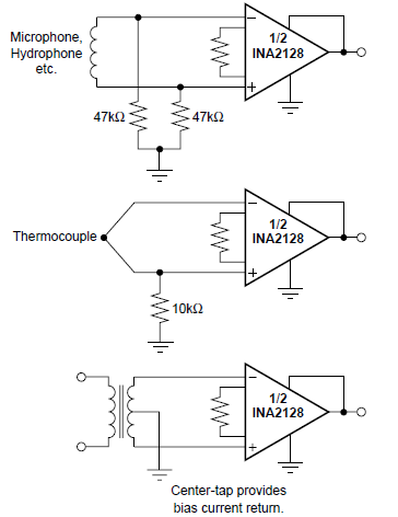
 Figure 7-3 Providing an Input Common-Mode
Current Path