ZHCSFN9G August   2008  – December 2015 INA219

PRODUCTION DATA.  

  1. 特性
  2. 应用范围
  3. 说明
  4. 修订历史记录
  5. Related Products
  6. Pin Configuration and Functions
  7. Specifications
    1. 7.1 Absolute Maximum Ratings
    2. 7.2 ESD Ratings
    3. 7.3 Recommended Operating Conditions
    4. 7.4 Thermal Information
    5. 7.5 Electrical Characteristics:
    6. 7.6 Bus Timing Diagram Definitions
    7. 7.7 Typical Characteristics
  8. Detailed Description
    1. 8.1 Overview
    2. 8.2 Functional Block Diagram
    3. 8.3 Feature Description
      1. 8.3.1 Basic ADC Functions
        1. 8.3.1.1 Power Measurement
        2. 8.3.1.2 PGA Function
        3. 8.3.1.3 Compatibility With TI Hot Swap Controllers
    4. 8.4 Device Functional Modes
      1. 8.4.1 Filtering and Input Considerations
    5. 8.5 Programming
      1. 8.5.1 Programming the Calibration Register
      2. 8.5.2 Programming the Power Measurement Engine
        1. 8.5.2.1 Calibration Register and Scaling
      3. 8.5.3 Simple Current Shunt Monitor Usage (No Programming Necessary)
      4. 8.5.4 Default Settings
      5. 8.5.5 Bus Overview
        1. 8.5.5.1 Serial Bus Address
        2. 8.5.5.2 Serial Interface
      6. 8.5.6 Writing to and Reading from the INA219
        1. 8.5.6.1 High-Speed I2C Mode
        2. 8.5.6.2 Power-Up Conditions
    6. 8.6 Register Maps
      1. 8.6.1 Register Information
      2. 8.6.2 Register Details
        1. 8.6.2.1 Configuration Register (address = 00h) [reset = 399Fh]
      3. 8.6.3 Data Output Registers
        1. 8.6.3.1 Shunt Voltage Register (address = 01h)
        2. 8.6.3.2 Bus Voltage Register (address = 02h)
        3. 8.6.3.3 Power Register (address = 03h) [reset = 00h]
        4. 8.6.3.4 Current Register (address = 04h) [reset = 00h]
      4. 8.6.4 Calibration Register
        1. 8.6.4.1 Calibration Register (address = 05h) [reset = 00h]
  9. Application and Implementation
    1. 9.1 Application Information
    2. 9.2 Typical Application
      1. 9.2.1 Design Requirements
      2. 9.2.2 Detailed Design Procedure
        1. 9.2.2.1 Register Results for the Example Circuit
  10. 10Power Supply Recommendations
  11. 11Layout
    1. 11.1 Layout Guidelines
    2. 11.2 Layout Example
  12. 12器件和文档支持
    1. 12.1 社区资源
    2. 12.2 商标
    3. 12.3 静电放电警告
    4. 12.4 Glossary
  13. 13机械、封装和可订购信息

封装选项

机械数据 (封装 | 引脚)
散热焊盘机械数据 (封装 | 引脚)
订购信息

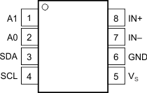
Pin Configuration and Functions

DCN Package
8-Pin SOT-23
Top View
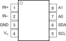
INA219 po_sot23_bos448.gif
D Package
8-Pin SOIC
Top View
INA219 po_so8_bos448.gif

Pin Functions

PIN I/O DESCRIPTION
NAME SOT-23 SOIC
IN+ 1 8 Analog Input Positive differential shunt voltage. Connect to positive side of shunt resistor.
IN– 2 7 Analog Input Negative differential shunt voltage. Connect to negative side of shunt resistor. Bus voltage is measured from this pin to ground.
GND 3 6 Analog Ground
VS 4 5 Analog Power supply, 3 to 5.5 V
SCL 5 4 Digital Input Serial bus clock line
SDA 6 3 Digital I/O Serial bus data line
A0 7 2 Digital Input Address pin. Table 1 shows pin settings and corresponding addresses.
A1 8 1 Digital Input Address pin. Table 1 shows pin settings and corresponding addresses.