ZHCSJE3C february   2019  – august 2021 INA191 , INA2191

PRODUCTION DATA  

  1.   1
  2. 特性
  3. 应用
  4. 说明
  5. Revision History
  6. Pin Configuration and Functions
  7. Specifications
    1. 6.1 Absolute Maximum Ratings
    2. 6.2 ESD Ratings
    3. 6.3 Recommended Operating Conditions
    4. 6.4 Thermal Information
    5. 6.5 Electrical Characteristics
    6. 6.6 Typical Characteristics
  8. Detailed Description
    1. 7.1 Overview
    2. 7.2 Functional Block Diagram
    3. 7.3 Feature Description
      1. 7.3.1 Precision Current Measurement
      2. 7.3.2 Low Input Bias Current
      3. 7.3.3 Low Quiescent Current With Output Enable
      4. 7.3.4 Bidirectional Current Monitoring (INA2191 Only)
      5. 7.3.5 High-Side and Low-Side Current Sensing
      6. 7.3.6 High Common-Mode Rejection
      7. 7.3.7 Rail-to-Rail Output Swing
    4. 7.4 Device Functional Modes
      1. 7.4.1 Normal Operation
      2. 7.4.2 Unidirectional Mode
      3. 7.4.3 Bidirectional Mode (INA2191 Only)
      4. 7.4.4 Input Differential Overload
      5. 7.4.5 Shutdown
  9. Application and Implementation
    1. 8.1 Application Information
      1. 8.1.1 Basic Connections
      2. 8.1.2 RSENSE and Device Gain Selection
      3. 8.1.3 Signal Conditioning
      4. 8.1.4 Common-Mode Voltage Transients
    2. 8.2 Typical Application
      1. 8.2.1 Microamp Current Measurement
        1. 8.2.1.1 Design Requirements
        2. 8.2.1.2 Detailed Design Procedure
        3. 8.2.1.3 Application Curve
  10. Power Supply Recommendations
  11. 10Layout
    1. 10.1 Layout Guidelines
    2. 10.2 Layout Examples
  12. 11Device and Documentation Support
    1. 11.1 Documentation Support
      1. 11.1.1 Related Documentation
    2. 11.2 接收文档更新通知
    3. 11.3 支持资源
    4. 11.4 Trademarks
    5. 11.5 静电放电警告
    6. 11.6 术语表
  13. 12Mechanical, Packaging, and Orderable Information

封装选项

请参考 PDF 数据表获取器件具体的封装图。

机械数据 (封装 | 引脚)
  • YBJ|12
散热焊盘机械数据 (封装 | 引脚)
订购信息

Shutdown

The INAx191 features an active-high ENABLE pin(s) that shuts down the device when pulled to ground. When the device is shut down, the quiescent current is reduced to 10 nA per channel (typical), the input bias currents are further reduced, and the disabled output goes to a high-impedance state. When disabled, the low quiescent and input currents extend the battery lifetime when the current measurement is not needed. When the ENABLE pin is driven above the enable threshold voltage, the device turns back on. When enabled, the typical output settling time is 130 µs.

The output of the INAx191 goes to a high-impedance state when disabled; therefore, it is possible to connect multiple outputs of the INAx191 together to a single ADC or measurement device, as shown in Figure 7-7. When connected in this way, enable only one INAx191 at a time, and make sure both devices have the same supply voltage. Using the INA2191 with the same approach as shown in Figure 7-7 provides the capability to monitor two currents with a single device.
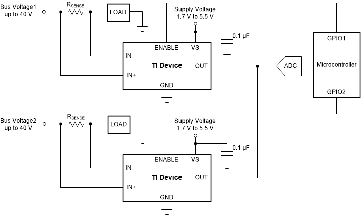
GUID-20210129-CA0I-WBQP-6S2X-FPMFWFX5XPNF-low.gif Figure 7-7 Multiplexing Multiple Devices With the ENABLE Pin