ZHCSDE7A February   2015  – March 2021 INA225-Q1

PRODUCTION DATA  

  1. 特性
  2. 应用
  3. 说明
  4. Revision History
  5. Pin Configuration and Functions
  6. Specifications
    1. 6.1 Absolute Maximum Ratings (1)
    2. 6.2 ESD Ratings
    3. 6.3 Recommended Operating Conditions
    4. 6.4 Thermal Information
    5. 6.5 Electrical Characteristics
    6. 6.6 Typical Characteristics
  7. Detailed Description
    1. 7.1 Overview
    2. 7.2 Functional Block Diagram
    3. 7.3 Feature Description
      1. 7.3.1 Selecting A Shunt Resistor
        1. 7.3.1.1 Selecting A Current-Sense Resistor Example
        2. 7.3.1.2 Optimizing Power Dissipation versus Measurement Accuracy
      2. 7.3.2 Programmable Gain Select
    4. 7.4 Device Functional Modes
      1. 7.4.1 Input Filtering
      2. 7.4.2 Shutting Down the Device
      3. 7.4.3 Using the Device with Common-Mode Transients Above 36 V
  8. Applications and Implementation
    1. 8.1 Application Information
    2. 8.2 Typical Applications
      1. 8.2.1 Microcontroller-Configured Gain Selection
        1. 8.2.1.1 Design Requirements
        2. 8.2.1.2 Detailed Design Procedure
        3. 8.2.1.3 Application Curve
      2. 8.2.2 Unidirectional Operation
        1. 8.2.2.1 Design Requirements
        2. 8.2.2.2 Detailed Design Procedure
        3. 8.2.2.3 Application Curve
      3. 8.2.3 Bidirectional Operation
        1. 8.2.3.1 Design Requirements
        2. 8.2.3.2 Detailed Design Procedure
        3. 8.2.3.3 Application Curve
  9. Power Supply Recommendations
  10. 10Layout
    1. 10.1 Layout Guidelines
    2. 10.2 Layout Example
  11. 11Device and Documentation Support
    1. 11.1 Documentation Support
      1. 11.1.1 Related Documentation
    2. 11.2 接收文档更新通知
    3. 11.3 支持资源
    4. 11.4 Trademarks
    5. 11.5 静电放电警告
    6. 11.6 术语表
  12. 12Mechanical, Packaging, and Orderable Information

封装选项

机械数据 (封装 | 引脚)
散热焊盘机械数据 (封装 | 引脚)
订购信息

Application Curve

Figure 8-2 illustrates how the microcontroller can monitor the ADC measurements to determine if the device gain setting should be adjusted to ensure the output of the device remains within the linear output range as well as the linear input range of the ADC. When the output of the device rises to a level near the desired maximum voltage level, the microcontroller can change the GPIO settings connected to the G0 and G1 gain-select terminals to adjust the device gain setting, thus resulting in the output voltage dropping to a lower output range. When the input current increases, the output voltage increases again to the desired maximum voltage level. The microcontroller can again change the device gain setting to drop the output voltage back to a lower range.
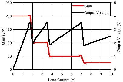
GUID-4F5F9706-D440-4155-81A1-FDF10C91CA30-low.pngFigure 8-2 Microcontroller-Configured Gain Selection Response