ZHCSL81A May 2020 – June 2021 INA229-Q1
PRODUCTION DATA
- 1 特性
- 2 应用
- 3 说明
- 4 Revision History
- 5 Pin Configuration and Functions
- 6 Specifications
-
7 Detailed Description
- 7.1 Overview
- 7.2 Functional Block Diagram
- 7.3 Feature Description
- 7.4 Device Functional Modes
- 7.5 Programming
- 7.6 Register Maps
- 8 Application and Implementation
- 9 Power Supply Recommendations
- 10Layout
- 11Device and Documentation Support
- 12Mechanical, Packaging, and Orderable Information
8.1.4 Input Filtering Considerations
As previously discussed, INA229-Q1 offers several options for noise filtering by allowing the user to select the conversion times and number of averages independently in the ADC_CONFIG register. The conversion times can be set independently for the shunt voltage and bus voltage measurements to allow added flexibility in monitoring of the power-supply bus.
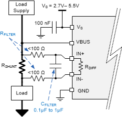
The internal ADC has good inherent noise rejection; however, the transients that occur at or very close to the sampling rate harmonics can cause problems. Because these signals are at 1 MHz and higher, they can be managed by incorporating filtering at the input of the device. Filtering high frequency signals enables the use of low-value series resistors on the filter with negligible effects on measurement accuracy. For best results, filter using the lowest possible series resistance (typically 100 Ω or less) and a ceramic capacitor. Recommended values for this capacitor are between 0.1 µF and 1 µF. Figure 8-1 shows the device with a filter added at the input.
Overload conditions are another consideration for the device inputs. The device inputs are specified to tolerate ±40 V differential across the IN+ and IN– pins. A large differential scenario might be a short to ground on the load side of the shunt. This type of event can result in full power-supply voltage across the shunt (as long the power supply or energy storage capacitors support it). Removing a short to ground can result in inductive kickbacks that could exceed the 40-V differential or 85-V common-mode absolute maximum rating of the device. Inductive kickback voltages are best controlled by Zener-type transient-absorbing devices (commonly called transzorbs) combined with sufficient energy storage capacitance. See the Transient Robustness for Current Shunt Monitors reference design which describes a high-side current shunt monitor used to measure the voltage developed across a current-sensing resistor when current passes through it.
In applications that do not have large energy storage, electrolytic capacitors on one or both sides of the shunt, an input overstress condition may result from an excessive dV/dt of the voltage applied to the input. A hard physical short is the most likely cause of this event. This problem occurs because an excessive dV/dt can activate the ESD protection in the device in systems where large currents are available. Testing demonstrates that the addition of 10-Ω resistors in series with each input of the device sufficiently protects the inputs against this dV/dt failure up to the 40-V maximum differential voltage rating of the device. Selecting these resistors in the range noted has minimal effect on accuracy.
 Figure 8-1 Input
Filtering
Figure 8-1 Input
FilteringDo not use values greater than 100 ohms for RFILTER. Doing so will degrade gain error and increase non-linearity.