ZHCSL81A May 2020 – June 2021 INA229-Q1
PRODUCTION DATA
- 1 特性
- 2 应用
- 3 说明
- 4 Revision History
- 5 Pin Configuration and Functions
- 6 Specifications
-
7 Detailed Description
- 7.1 Overview
- 7.2 Functional Block Diagram
- 7.3 Feature Description
- 7.4 Device Functional Modes
- 7.5 Programming
- 7.6 Register Maps
- 8 Application and Implementation
- 9 Power Supply Recommendations
- 10Layout
- 11Device and Documentation Support
- 12Mechanical, Packaging, and Orderable Information
7.3.1 Versatile High Voltage Measurement Capability
The INA229-Q1 operates off a 2.7 V to 5.5 V supply but can measure voltage and current on rails as high as 85 V. The current is measured by sensing the voltage drop across a external shunt resistor at the IN+ and IN– pins. The input stage of the INA229-Q1 is designed such that the input common-mode voltage can be higher than the device supply voltage, VS. The supported common-mode voltage range at the input pins is –0.3 V to +85 V, which makes the device well suited for both high-side and low-side current measurements. There are no special considerations for power-supply sequencing because the common-mode input range and device supply voltage are independent of each other; therefore, the bus voltage can be present with the supply voltage off, and vice-versa without damaging the device.
The device also measures the bus supply voltage through the VBUS pin and temperature through the integrated temperature sensor. The differential shunt voltage is measured between the IN+ and IN– pins, while the bus voltage is measured with respect to device ground. Monitored bus voltages can range from 0 V to 85 V, while monitored temperatures can range from -40 ºC to +125 ºC.
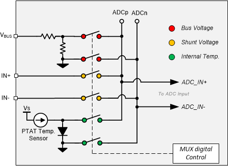
Shunt voltage, bus voltage, and temperature measurements are multiplexed internally to a single ADC as shown in Figure 7-1.
 Figure 7-1 High-Voltage
Input Multiplexer