ZHCS766A February 2012 – December 2021 INA230
PRODUCTION DATA
- 1 特性
- 2 应用
- 3 说明
- 4 Revision History
- 5 Related Products
- 6 Pin Configuration and Functions
- 7 Specifications
-
8 Detailed Description
- 8.1 Overview
- 8.2 Functional Block Diagram
- 8.3 Feature Description
- 8.4 Device Functional Modes
- 8.5 Programming
- 8.6
Register Maps
- 8.6.1 Configuration Register (00h, Read/Write)
- 8.6.2 AVG Bit Settings [11:9]
- 8.6.3 VBUS CT Bit Settings [8:6]
- 8.6.4 VSH CT Bit Settings [5:3]
- 8.6.5 Mode Settings [2:0]
- 8.6.6
Data Output Register
- 8.6.6.1 Shunt Voltage Register (01h, Read-Only)
- 8.6.6.2 Bus Voltage Register (02h, Read-Only) (1)
- 8.6.6.3 Power Register (03h, Read-Only)
- 8.6.6.4 Current Register (04h, Read-Only)
- 8.6.6.5 Calibration Register (05h, Read/Write)
- 8.6.6.6 Mask/Enable Register (06h, Read/Write)
- 8.6.6.7 Alert Limit Register (07h, Read/Write)
- 9 Application and Implementation
- 10Power Supply Recommendations
- 11Layout
- 12Device and Documentation Support
- 13Mechanical, Packaging, and Orderable Information
封装选项
机械数据 (封装 | 引脚)
散热焊盘机械数据 (封装 | 引脚)
- RGT|16
订购信息
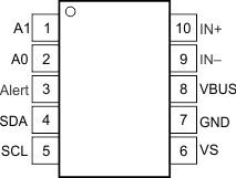
6 Pin Configuration and Functions
Figure 6-1 RGT Package16-Pin VQFN(Top View)
 Figure 6-2 DGS Package10-Pin VSSOP(Top View)
Table 6-1 Pin Functions
| PIN | TYPE | DESCRIPTION | ||
|---|---|---|---|---|
| NAME | VQFN | VSSOP | ||
| A0 | 2 | 2 | Digital input | Address pin. Connect to GND, SCL, SDA, or VS. Table 8-2 shows pin settings and corresponding addresses. |
| A1 | 1 | 1 | Digital input | Address pin. Connect to GND, SCL, SDA, or VS. Table 8-2 shows pin settings and corresponding addresses. |
| ALERT | 3 | 3 | Digital output | Multi-functional alert, open-drain output. |
| GND | 10 | 7 | Analog | Ground |
| NC | 6, 7, 8, 14, 15, 16 | — | — | No internal connection |
| SCL | 5 | 5 | Digital input | Serial bus clock line, open-drain input. |
| SDA | 4 | 4 | Digital input/output | Serial bus data line, open-drain input/output. |
| VBUS | 11 | 8 | Analog input | Bus voltage input |
| IN– | 12 | 9 | Analog input | Negative differential shunt voltage input. For high-side applications, connect to load side of sense resistor. For low-side applications, connect to ground side of sense resistor. |
| IN+ | 13 | 10 | Analog input | Positive differential shunt voltage input. For high-side applications, connect to bus voltage side of sense resistor. For low-side applications, connect to load side of sense resistor. |
| VS | 9 | 6 | Analog | Power supply, 2.7 V to 5.5 V. |
| Thermal Pad | — | PAD | — | This pad can be connected to ground or left floating. |