ZHCSAQ1D February 2013 – July 2022 INA231
PRODUCTION DATA
- 1 特性
- 2 应用
- 3 说明
- 4 Revision History
- 5 Device Comparison
- 6 Pin Configuration and Functions
- 7 Specifications
-
8 Detailed Description
- 8.1 Overview
- 8.2 Functional Block Diagram
- 8.3 Feature Description
- 8.4 Device Functional Modes
- 8.5 Programming
- 8.6
Register Maps
- 8.6.1 Configuration Register (00h, Read/Write)
- 8.6.2 Shunt Voltage Register (01h, Read-Only)
- 8.6.3 Bus Voltage Register (02h, Read-Only)
- 8.6.4 Power Register (03h, Read-Only)
- 8.6.5 Current Register (04h, Read-Only)
- 8.6.6 Calibration Register (05h, Read/Write)
- 8.6.7 Mask/Enable Register (06h, Read/Write)
- 8.6.8 Alert Limit Register (07h, Read/Write)
- 9 Application and Implementation
- 10Device and Documentation Support
- 11Mechanical, Packaging, and Orderable Information
封装选项
请参考 PDF 数据表获取器件具体的封装图。
机械数据 (封装 | 引脚)
- YFF|12
- YFD|12
散热焊盘机械数据 (封装 | 引脚)
订购信息
8.4.1 Averaging and Conversion Time Considerations
The INA231 has programmable conversion times for both the shunt voltage and bus voltage measurements. The conversion times for these measurements can be selected from as fast as 140 μs to as long as 8.244 ms. The conversion time settings, along with the programmable averaging mode, allow the INA231 to be configured to optimize the available timing requirements in a given application. For example, if a system requires that data be read every 5 ms, the INA231 can be configured with the conversion times set to 588 μs and the averaging mode set to 4. This configuration results in the data updating approximately every 4.7 ms. The INA231 can also be configured with a different conversion time setting for the shunt and bus voltage measurements. This type of approach is common in applications where the bus voltage tends to be relatively stable. This situation allows for the time spent measuring the bus voltage to be reduced relative to the shunt voltage measurement. The shunt voltage conversion time can be set to 4.156 ms with the bus voltage conversion time set to 588 μs, and the averaging mode set to 1. This configuration also results in data updating approximately every 4.7 ms.
There are trade-offs associated with the conversion time settings and the averaging mode used. The averaging feature can significantly improve the measurement accuracy by effectively filtering the signal. This approach allows the INA231 to reduce noise in the measurement that may be caused by noise coupling into the signal. A greater number of averages enables the INA231 to be more effective in reducing the noise component of the measurement.
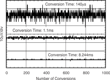
The conversion times selected can also have an impact on the measurement accuracy; this effect can be seen in Figure 8-3. Multiple conversion times are shown to illustrate the impact of noise on the measurement. In order to achieve the highest accuracy measurement possible, use a combination of the longest allowable conversion times and highest number of averages, based on the timing requirements of the system.
 Figure 8-3 Noise vs Conversion Time