ZHCSLF9A June   2020  – June 2021 INA237-Q1

PRODUCTION DATA  

  1. 特性
  2. 应用
  3. 说明
  4. Revision History
  5. Pin Configuration and Functions
  6. Specifications
    1. 6.1 Absolute Maximum Ratings
    2. 6.2 ESD Ratings
    3. 6.3 Recommended Operating Conditions
    4. 6.4 Thermal Information
    5. 6.5 Electrical Characteristics
    6. 6.6 Timing Requirements (I2C)
    7. 6.7 Timing Diagram
    8. 6.8 Typical Characteristics
  7. Detailed Description
    1. 7.1 Overview
    2. 7.2 Functional Block Diagram
    3. 7.3 Feature Description
      1. 7.3.1 Versatile High Voltage Measurement Capability
      2. 7.3.2 Power Calculation
      3. 7.3.3 Low Bias Current
      4. 7.3.4 High-Precision Delta-Sigma ADC
        1. 7.3.4.1 Low Latency Digital Filter
        2. 7.3.4.2 Flexible Conversion Times and Averaging
      5. 7.3.5 Integrated Precision Oscillator
      6. 7.3.6 Multi-Alert Monitoring and Fault Detection
    4. 7.4 Device Functional Modes
      1. 7.4.1 Shutdown Mode
      2. 7.4.2 Power-On Reset
    5. 7.5 Programming
      1. 7.5.1 I2C Serial Interface
        1. 7.5.1.1 Writing to and Reading Through the I2C Serial Interface
        2. 7.5.1.2 High-Speed I2C Mode
        3. 7.5.1.3 SMBus Alert Response
    6. 7.6 Register Maps
      1. 7.6.1 INA237-Q1 Registers
  8. Application and Implementation
    1. 8.1 Application Information
      1. 8.1.1 Device Measurement Range and Resolution
      2. 8.1.2 Current and Power Calculations
      3. 8.1.3 ADC Output Data Rate and Noise Performance
      4. 8.1.4 Input Filtering Considerations
    2. 8.2 Typical Application
      1. 8.2.1 Design Requirements
      2. 8.2.2 Detailed Design Procedure
        1. 8.2.2.1 Select the Shunt Resistor
        2. 8.2.2.2 Configure the Device
        3. 8.2.2.3 Program the Shunt Calibration Register
        4. 8.2.2.4 Set Desired Fault Thresholds
        5. 8.2.2.5 Calculate Returned Values
      3. 8.2.3 Application Curves
  9. Power Supply Recommendations
  10. 10Layout
    1. 10.1 Layout Guidelines
    2. 10.2 Layout Example
  11. 11Device and Documentation Support
    1. 11.1 接收文档更新通知
    2. 11.2 支持资源
    3. 11.3 Trademarks
    4. 11.4 Electrostatic Discharge Caution
    5. 11.5 术语表
  12. 12Mechanical, Packaging, and Orderable Information

封装选项

机械数据 (封装 | 引脚)
散热焊盘机械数据 (封装 | 引脚)
订购信息

Typical Characteristics

at TA = 25 °C, VVS = 3.3 V, VCM = 48 V, VSENSE = 0, and VVBUS = 48 V (unless otherwise noted)
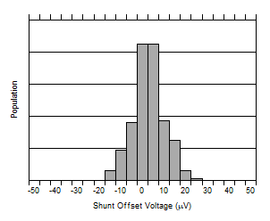
GUID-20210212-CA0I-HHFQ-QKVS-X04HFHRSTD7K-low.gif
VCM = 48 V
Figure 6-2 Shunt Input Offset Voltage Production Distribution
Figure 6-4 Shunt Input Offset Voltage vs. Temperature
Figure 6-6 Shunt Input Common-Mode Rejection Ratio vs. Temperature
VCM = 24 V
Figure 6-8 Shunt Input Gain Error vs. Temperature
GUID-20210212-CA0I-6PHJ-P6QK-XLLX1DTGBF0M-low.gif
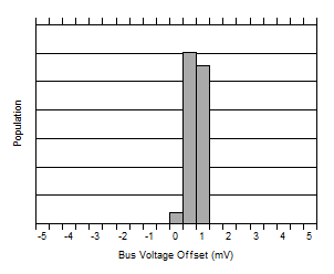
VVBUS = 20 mV
Figure 6-10 Bus Input Offset Voltage Production Distribution
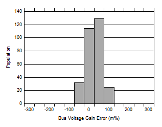
GUID-20210212-CA0I-WRQD-P3M2-XLSXV1NKWJ1B-low.gifFigure 6-12 Bus Input Gain Error Production Distribution
Figure 6-14 Input Bias Current vs. Differential Input Voltage
Figure 6-16 Input Bias Current vs. Temperature
Figure 6-18 Active IQ vs. Temperature
Figure 6-20 Shutdown IQ vs. Supply Voltage
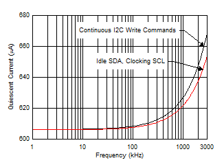
GUID-20210105-CA0I-SKM5-TJV3-VJXJ8XVFDN9R-low.gifFigure 6-22 Active IQ vs. Clock Frequency
Figure 6-24 Internal Clock Frequency vs. Power Supply
GUID-20210212-CA0I-776N-RT4T-8QLK53MKFF7G-low.gif
VCM = 0 V
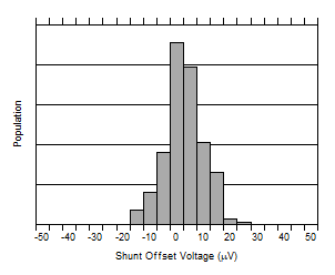
Figure 6-3 Shunt Input Offset Voltage Production Distribution
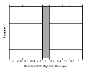
GUID-20210212-CA0I-DH1F-Z2TS-LZNRZ8ZHT62P-low.gifFigure 6-5 Common-Mode Rejection Ratio Production Distribution
GUID-20210212-CA0I-V2PS-HRFR-SCP4H07FWHXS-low.gif
VCM = 24 V
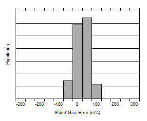
Figure 6-7 Shunt Input Gain Error Production Distribution
Figure 6-9 Shunt Input Gain Error vs. Common-Mode Voltage
VVBUS = 20 mV
Figure 6-11 Bus Input Offset Voltage vs. Temperature
Figure 6-13 Bus Input Gain Error vs. Temperature
Figure 6-15 Input Bias Current (IB+ or IB–) vs. Common-Mode Voltage
Figure 6-17 Input Bias Current vs. Temperature, Shutdown
Figure 6-19 Active IQ vs. Supply Voltage
Figure 6-21 Shutdown IQ vs. Temperature
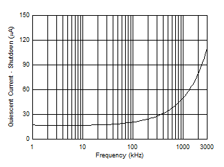
GUID-20210105-CA0I-8DDR-NSL7-DBN6WDC3VT3J-low.gifFigure 6-23 Shutdown IQ vs. Clock Frequency
Figure 6-25 Internal Clock Frequency vs. Temperature