ZHCSL82A May 2020 – June 2021 INA239-Q1
PRODUCTION DATA
- 1 特性
- 2 应用
- 3 说明
- 4 Revision History
- 5 Pin Configuration and Functions
- 6 Specifications
-
7 Detailed Description
- 7.1 Overview
- 7.2 Functional Block Diagram
- 7.3 Feature Description
- 7.4 Device Functional Modes
- 7.5 Programming
- 7.6 Register Maps
- 8 Application and Implementation
- 9 Power Supply Recommendations
- 10Layout
- 11Device and Documentation Support
- 12Mechanical, Packaging, and Orderable Information
7.3.6 Multi-Alert Monitoring and Fault Detection
The INA239-Q1 includes a multipurpose, open-drain ALERT output pin that can be used to report multiple diagnostics or as an indicator that the ADC conversion is complete when the device is operating in both triggered and continuous conversion mode. The diagnostics listed in Table 7-1 are constantly monitored and can be reported through the ALERT pin whenever the monitored output value crosses its associated out-of-range threshold.
| INA239-Q1 DIAGNOSTIC | STATUS BIT IN DIAG_ALRT REGISTER (RO) | OUT-OF-RANGE THRESHOLD REGISTER (R/W) | REGISTER DEFAULT VALUE |
|---|---|---|---|
| Shunt Under Voltage Limit | SHNTUL | SUVL | 0x8000 h (two's complement) |
| Shunt Over Voltage Limit | SHNTOL | SOVL | 0x7FFF h (two's complement) |
| Bus Voltage Over-Limit | BUSOL | BOVL | 0x7FFF h (two's complement, positive values only) |
| Bus Voltage Under-Limit | BUSUL | BUVL | 0x0000 h (two's complement, positive values only) |
| Temperature Over-Limit | TMPOL | TEMP_LIMIT | 0xFFFF h (two's complement, positive values only) |
| Power Over-Limit | POL | PWR_LIMIT | 0x7FFF h (two's complement) |
A read of the DIAG_ALRT register is used to determine which diagnostic has triggered the ALERT pin. This register, shown in Table 7-13, is also used to monitor other associated diagnostics as well as configure some ALERT pin functions.
- Alert latch enable — In case the ALERT pin is triggered, this function will hold the value of the pin even after all diagnostic conditions have cleared. A read of the DIAG_ALRT register will reset the status of the ALERT pin. This function is enabled by setting the ALATCH bit.
- Conversion ready enable — Enables the ALERT pin to assert when an ADC conversion has completed and output values are ready to be read through the digital interface. This function is enabled by setting the CNVR bit. The conversion completed events can also be read through the CNVRF bit regardless of the CNVR bit setting.
- Alert comparison on averaged output — Allows the out-of-range threshold value to be compared to the averaged data values produced by the ADC. This helps to additionally remove noise from the output data when compared to the out-of-range threshold to avoid false alerts due to noise. However, the diagnostic will be delayed due to the time needed for averaging. This function is enabled by setting the SLOWALERT bit.
- Alert polarity — Allows the device to invert the active state of the ALERT pin. Note that the ALERT pin is an open-drain output that must be pulled-up by a resistor. The ALERT pin is active-low by default and can be configured for active high function using the APOL control bit.
Other diagnostic functions that are not reported by the ALERT pin but are available by reading the DIAG_ALRT register:
- Math overflow — Indicated by the MATHOF bit, reports when an arithmetic operation has caused an internal register overflow.
- Memory status — Indicated by the MEMSTAT bit, monitors the health of the device non-volatile trim memory. This bit should always read '1' when the device is operating properly.
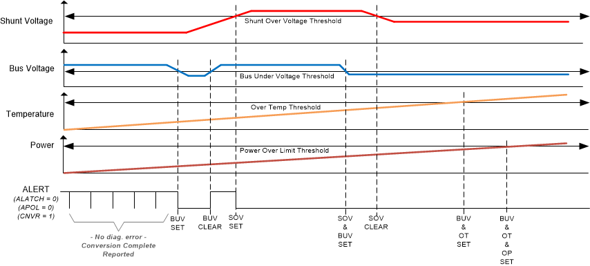
When the ALERT pin is configured to report the ADC conversion complete event, the ALERT pin becomes a multipurpose reporting output. Figure 7-6 shows an example where the device reports ADC conversion complete events while the INA239-Q1 device is subject to shunt over voltage (over current) event, bus under voltage event, over temperature event and over power-limit event.
 Figure 7-6 Multi-Alert
Configuration