ZHCSFO8C July 2016 – September 2023 INA250-Q1
PRODUCTION DATA
- 1
- 1 特性
- 2 应用
- 3 说明
- 4 Revision History
- 5 Pin Configuration and Functions
- 6 Specifications
- 7 Detailed Description
- 8 Applications and Implementation
- 9 Device and Documentation Support
- 10Mechanical, Packaging, and Orderable Information
7.4.3 Shutting Down the Device
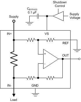
Although the device does not have a shutdown pin, the low power consumption allows for the device to be powered from the output of a logic gate or transistor switch that may turn on and turn off the voltage connected to the device power-supply pin. However, in current-shunt monitoring applications, there is also a concern for how much current is drained from the shunt circuit in shutdown conditions. Evaluating this current drain involves considering the simplified schematic in shutdown mode, as shown in Figure 7-6.
 Figure 7-6 Shutting Down the Device
Note that there is typically an approximate 1-MΩ impedance (from the combination of the feedback and input resistors) from each device input to the REF pin. The amount of current flowing through these pins depends on the respective configuration. For example, if the REF pin is grounded, calculating the effect of the 1-MΩ impedance from the shunt to ground is straightforward. However, if the reference or op amp is powered when the device is shut down, the calculation is direct. Instead of assuming 1 MΩ to ground, assume 1 MΩ to the reference voltage. If the reference or op amp is also shut down, some knowledge of the reference or op amp output impedance under shutdown conditions is required. For instance, if the reference source functions similar to an open circuit when un-powered, little or no current flows through the 1-MΩ path.