ZHCSFO8C July 2016 – September 2023 INA250-Q1
PRODUCTION DATA
- 1
- 1 特性
- 2 应用
- 3 说明
- 4 Revision History
- 5 Pin Configuration and Functions
- 6 Specifications
- 7 Detailed Description
- 8 Applications and Implementation
- 9 Device and Documentation Support
- 10Mechanical, Packaging, and Orderable Information
7.4.4 Using the Device with Common-Mode Transients Above 36 V
With a small amount of additional circuitry, the
device may be used in circuits subject to transients higher than
36 V (such as in automotive applications). Use only
zener diodes or zener-type transient absorbers (sometimes referred to as
transzorbs); any other type of transient absorber has an unacceptable
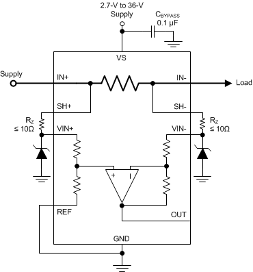
time delay. Start by adding a pair of resistors, as shown in Figure 7-7, as a working impedance for the zener. Keeping these resistors as small as
possible is preferable; a resistor value of 10-Ω is the most common. This value
limits the effect on accuracy with the addition of these external components, as
described in the Input Filtering section. Device interconnections between the shunt resistor and amplifier
have a current handling limit of 1 A. Using a 10-Ω resistor limits the allowable
transient range to 10 V above the zener clamp so the device is not damaged. Larger
resistor values may be used in this protection circuit to accommodate a larger
transient voltage range, which results in a larger effect on gain error. Because
this circuit limits only short-term transients, many applications are satisfied with
a 10-Ω resistor, along with conventional zener diodes of the lowest power rating
available.
 Figure 7-7 Device Transient Protection