ZHCSDO5C April   2015  – September 2023

PRODUCTION DATA  

  1.   1
  2. 特性
  3. 应用
  4. 说明
  5. Revision History
  6. Pin Configuration and Functions
  7. Specifications
    1. 6.1 Absolute Maximum Ratings
    2. 6.2 ESD Ratings
    3. 6.3 Recommended Operating Conditions
    4. 6.4 Thermal Information
    5. 6.5 Electrical Characteristics
    6. 6.6 Typical Characteristics
  8. Detailed Description
    1. 7.1 Overview
    2. 7.2 Functional Block Diagram
    3. 7.3 Feature Description
      1. 7.3.1 Integrated Shunt Resistor
      2. 7.3.2 Short-Circuit Duration
      3. 7.3.3 Temperature Stability
    4. 7.4 Device Functional Modes
      1. 7.4.1 Amplifier Operation
      2. 7.4.2 Input Filtering
        1. 7.4.2.1 Calculating Gain Error Resulting from External Filter Resistance
      3. 7.4.3 Shutting Down the Device
      4. 7.4.4 Using the Device with Common-Mode Transients Above 36 V
  9. Applications and Implementation
    1. 8.1 Application Information
    2. 8.2 Typical Applications
      1. 8.2.1 Current Summing
        1. 8.2.1.1 Design Requirements
        2. 8.2.1.2 Detailed Design Procedure
        3. 8.2.1.3 Application Curve
      2. 8.2.2 Parallel Multiple INA250 Devices for Higher Current
        1. 8.2.2.1 Design Requirements
        2. 8.2.2.2 Detailed Design Procedure
        3. 8.2.2.3 Application Curve
      3. 8.2.3 Current Differencing
        1. 8.2.3.1 Design Requirements
        2. 8.2.3.2 Detailed Design Procedure
        3. 8.2.3.3 Application Curve
    3. 8.3 Power Supply Recommendations
    4. 8.4 Layout
      1. 8.4.1 Layout Guidelines
      2. 8.4.2 Layout Examples
  10. Device and Documentation Support
    1. 9.1 Documentation Support
      1. 9.1.1 Related Documentation
    2. 9.2 接收文档更新通知
    3. 9.3 支持资源
    4. 9.4 Trademarks
    5. 9.5 静电放电警告
    6. 9.6 术语表
  11. 10Mechanical, Packaging, and Orderable Information

封装选项

机械数据 (封装 | 引脚)
散热焊盘机械数据 (封装 | 引脚)
订购信息

Typical Characteristics

At TA = 25°C, VS = 5 V, VIN+ = 12 V, VREF = 2.5 V, ISENSE = IN+ = 0 A, unless otherwise noted.
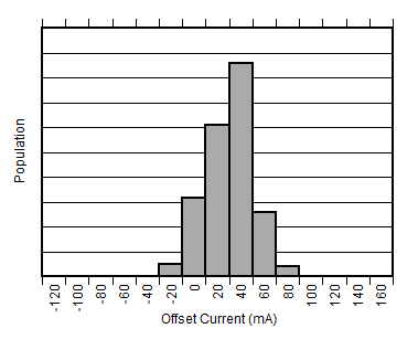
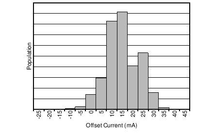
GUID-7ED724E9-9271-4738-9AC5-F7D27E431C0C-low.gif
Figure 6-1 INA250A1 Input Offset Distribution
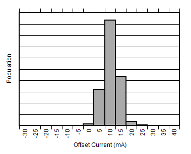
GUID-8DF469D7-B867-4116-A71C-0772793B9560-low.gif
Figure 6-3 INA250A3 Input Offset Distribution
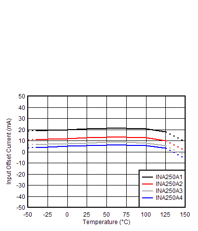
GUID-567DF807-8771-4CF4-9485-E3F16961B180-low.gif
Figure 6-5 Input Offset vs Temperature
GUID-22A71B3C-7320-453F-83E8-8BD769548542-low.png
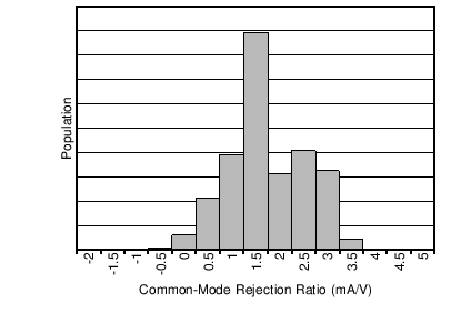
Figure 6-7 INA250A2 Common-Mode Rejection Ratio Distribution
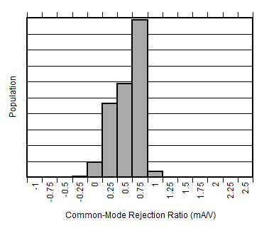
GUID-C744BCCB-C2C1-4F13-96B4-291DFF54E30D-low.gif
Figure 6-9 INA250A4 Common-Mode Rejection Ratio Distribution
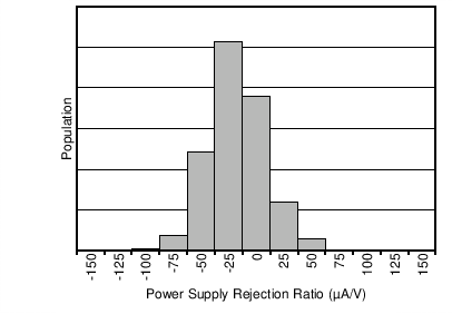
GUID-58EA1A13-83F0-4649-818B-56EE036974FF-low.png
Figure 6-11 Power-Supply Rejection Ratio Distribution
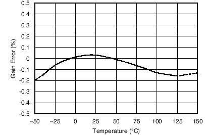
GUID-847B41E8-8A61-4AEF-B18D-C0BA9CABCC30-low.png
Figure 6-13 System Gain Error vs Temperature
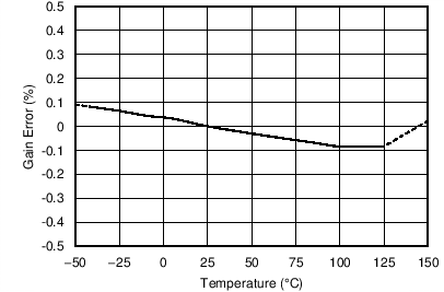
GUID-46997B79-E2EE-40D7-9E05-201A68828D97-low.png
Figure 6-15 Amplifier Gain Error vs Temperature
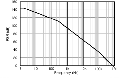
GUID-ABB13DFC-B2D7-47F7-B703-05D2F97DEBF7-low.png
VCM = 12 V, VREF = 2.5 V, ISENSE = 0 A, VS = 5 V + 250-mV sine disturbance
Figure 6-17 Power-Supply Rejection vs Frequency
GUID-AFF16CFB-305F-442D-83C9-8275B71B28E0-low.gif
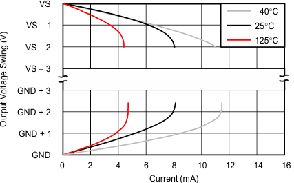
Figure 6-19 Output Voltage Swing vs Output Current
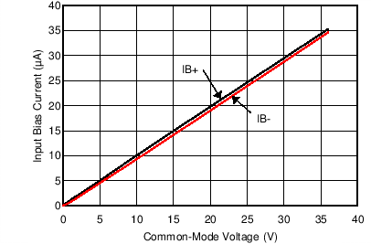
GUID-A8501B73-E0DD-4917-816C-A5754DFBE925-low.png
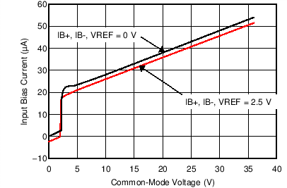
ISENSE = 0 A, VS = 0 V, VREF = 0 V
Figure 6-21 Input Bias Current vs Common-Mode Voltage (VS = 0 V)
GUID-CF36E2B6-8671-4B2A-A404-101FB39B0ABC-low.png
VREF = VS / 2
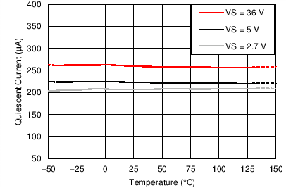
Figure 6-23 Quiescent Current vs Temperature
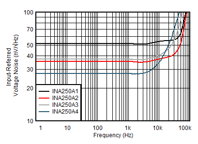
GUID-44CE8D59-BF11-4884-9754-5B927E299BC5-low.gif
VS = 5 V, VREF = 2.5 V, ISENSE = 0 A
Figure 6-25 Input-Referred Voltage Noise vs Frequency
GUID-53787B91-7336-4573-A69D-40738C18983D-low.gif
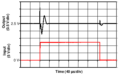
Input = (VIN+) - (VIN-)
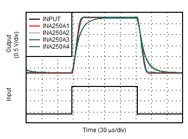
Figure 6-27 Step Response
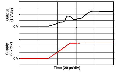
GUID-0062A8FF-B775-43C4-B477-D3B76B74D91C-low.png
Figure 6-29 Start-Up Response
GUID-DFA66BF9-780B-4DF9-8B27-087DD27EC744-low.png
Figure 6-2 INA250A2 Input Offset Distribution
GUID-44E98CEB-F0E1-416E-8B17-4A810078C09C-low.gif
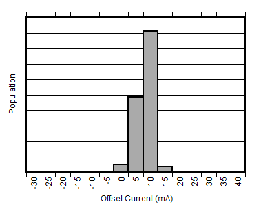
Figure 6-4 INA250A4 Input Offset Distribution
GUID-FC5F434E-B6E4-461E-83BD-F80F26940BCD-low.gif
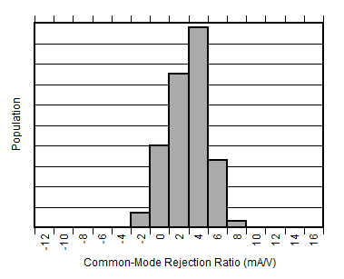
Figure 6-6 INA250A1 Common-Mode Rejection Ratio Distribution
GUID-69EB4E3D-FC27-4A6C-86E8-02E9B10168B9-low.gif
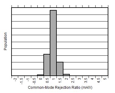
Figure 6-8 INA250A3 Common-Mode Rejection Ratio Distribution
GUID-3165B7BE-BF3D-4E06-932F-C04F41D5C0CB-low.gif
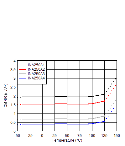
Figure 6-10 Common-Mode Rejection Ratio vs Temperature
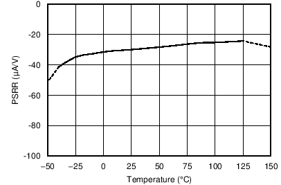
GUID-13AE2F0E-33DD-4EB4-B7AC-DC9995E703AD-low.png
Figure 6-12 Power-Supply Rejection Ratio vs Temperature
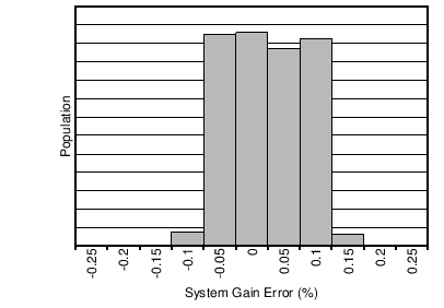
GUID-F6C5956B-DEAF-4F0C-9F18-88130BECC5AD-low.png
System gain error = RSHUNT error + amplifier gain error, load current = 10 A
Figure 6-14 System Gain Error Distribution
GUID-E1C04027-77A0-4F8A-8699-6365D1BD862A-low.gif
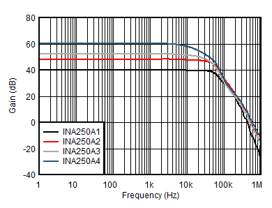
VCM = 12 V, ISENSE = 500 mAPP
Figure 6-16 Amplifier Gain vs Frequency
GUID-BAF6757A-FB5B-4B1C-A06C-EDA7BB237259-low.png
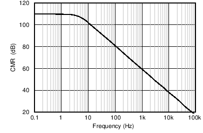
VS = 5 V, VREF = 2.5 V, ISENSE = 0 A, VCM = 1-V sine wave
Figure 6-18 Common-Mode Rejection vs Frequency
GUID-B59A9A4A-2F75-4011-AF3A-57FE709DEED4-low.png
ISENSE = 0 A, VS = 5 V
Figure 6-20 Input Bias Current vs Common-Mode Voltage (VS = 5 V)
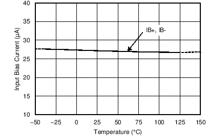
GUID-F6590D05-7125-4388-8242-4E48380C930C-low.png
ISENSE = 0 A, VS = 5 V
Figure 6-22 Input Bias Current vs Temperature
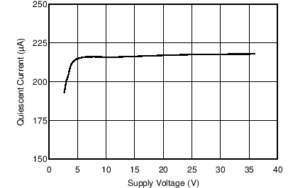
GUID-080C3394-D6B2-4E24-8DCA-59011DCC9BDE-low.png
VREF = 2.5 V
Figure 6-24 Quiescent Current vs Supply Voltage
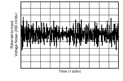
GUID-670777C6-F16D-4D70-A354-F74A82F4B228-low.png
VS = 5 V, VCM = 0 V, ISENSE = 0 A
Figure 6-26 0.1-Hz to 10-Hz Voltage Noise (Referred-to-Input)
GUID-A3296DCD-2477-4C2A-A265-6F0344E65FCE-low.png
Input = VIN+, VREF = 2.5 V
Figure 6-28 Common-Mode Transient Response