ZHCSDO5C April   2015  – September 2023

PRODUCTION DATA  

  1.   1
  2. 特性
  3. 应用
  4. 说明
  5. Revision History
  6. Pin Configuration and Functions
  7. Specifications
    1. 6.1 Absolute Maximum Ratings
    2. 6.2 ESD Ratings
    3. 6.3 Recommended Operating Conditions
    4. 6.4 Thermal Information
    5. 6.5 Electrical Characteristics
    6. 6.6 Typical Characteristics
  8. Detailed Description
    1. 7.1 Overview
    2. 7.2 Functional Block Diagram
    3. 7.3 Feature Description
      1. 7.3.1 Integrated Shunt Resistor
      2. 7.3.2 Short-Circuit Duration
      3. 7.3.3 Temperature Stability
    4. 7.4 Device Functional Modes
      1. 7.4.1 Amplifier Operation
      2. 7.4.2 Input Filtering
        1. 7.4.2.1 Calculating Gain Error Resulting from External Filter Resistance
      3. 7.4.3 Shutting Down the Device
      4. 7.4.4 Using the Device with Common-Mode Transients Above 36 V
  9. Applications and Implementation
    1. 8.1 Application Information
    2. 8.2 Typical Applications
      1. 8.2.1 Current Summing
        1. 8.2.1.1 Design Requirements
        2. 8.2.1.2 Detailed Design Procedure
        3. 8.2.1.3 Application Curve
      2. 8.2.2 Parallel Multiple INA250 Devices for Higher Current
        1. 8.2.2.1 Design Requirements
        2. 8.2.2.2 Detailed Design Procedure
        3. 8.2.2.3 Application Curve
      3. 8.2.3 Current Differencing
        1. 8.2.3.1 Design Requirements
        2. 8.2.3.2 Detailed Design Procedure
        3. 8.2.3.3 Application Curve
    3. 8.3 Power Supply Recommendations
    4. 8.4 Layout
      1. 8.4.1 Layout Guidelines
      2. 8.4.2 Layout Examples
  10. Device and Documentation Support
    1. 9.1 Documentation Support
      1. 9.1.1 Related Documentation
    2. 9.2 接收文档更新通知
    3. 9.3 支持资源
    4. 9.4 Trademarks
    5. 9.5 静电放电警告
    6. 9.6 术语表
  11. 10Mechanical, Packaging, and Orderable Information

封装选项

机械数据 (封装 | 引脚)
散热焊盘机械数据 (封装 | 引脚)
订购信息

Input Filtering

An obvious and straightforward location for filtering is at the device output; however, this location negates the advantage of the low output impedance of the output stage buffer. The input then represents the best location for implementing external filtering. Figure 7-4 shows the typical implementation of the input filter for the device.
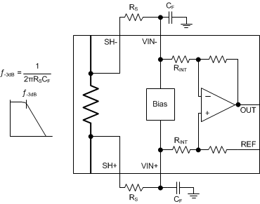
GUID-93A69556-C30B-4AE9-8739-F1127ED26E89-low.gifFigure 7-4 Input Filter

The addition of external series resistance at the input pins to the amplifier, however, creates an additional error in the measurement. Keep the value of these series resistors to 10 Ω or less, if possible, to reduce the affect to accuracy. The internal bias network illustrated in Figure 7-4 present at the input pins creates a mismatch in input bias currents when a differential voltage is applied between the input pins, as shown in Figure 7-5.
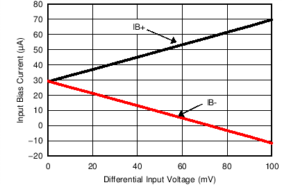
GUID-527B957B-1025-4DA7-A3FC-137F9B0279BB-low.pngFigure 7-5 Input Bias Current vs Differential Input Voltage