ZHCSDO5C April   2015  – September 2023

PRODUCTION DATA  

  1.   1
  2. 特性
  3. 应用
  4. 说明
  5. Revision History
  6. Pin Configuration and Functions
  7. Specifications
    1. 6.1 Absolute Maximum Ratings
    2. 6.2 ESD Ratings
    3. 6.3 Recommended Operating Conditions
    4. 6.4 Thermal Information
    5. 6.5 Electrical Characteristics
    6. 6.6 Typical Characteristics
  8. Detailed Description
    1. 7.1 Overview
    2. 7.2 Functional Block Diagram
    3. 7.3 Feature Description
      1. 7.3.1 Integrated Shunt Resistor
      2. 7.3.2 Short-Circuit Duration
      3. 7.3.3 Temperature Stability
    4. 7.4 Device Functional Modes
      1. 7.4.1 Amplifier Operation
      2. 7.4.2 Input Filtering
        1. 7.4.2.1 Calculating Gain Error Resulting from External Filter Resistance
      3. 7.4.3 Shutting Down the Device
      4. 7.4.4 Using the Device with Common-Mode Transients Above 36 V
  9. Applications and Implementation
    1. 8.1 Application Information
    2. 8.2 Typical Applications
      1. 8.2.1 Current Summing
        1. 8.2.1.1 Design Requirements
        2. 8.2.1.2 Detailed Design Procedure
        3. 8.2.1.3 Application Curve
      2. 8.2.2 Parallel Multiple INA250 Devices for Higher Current
        1. 8.2.2.1 Design Requirements
        2. 8.2.2.2 Detailed Design Procedure
        3. 8.2.2.3 Application Curve
      3. 8.2.3 Current Differencing
        1. 8.2.3.1 Design Requirements
        2. 8.2.3.2 Detailed Design Procedure
        3. 8.2.3.3 Application Curve
    3. 8.3 Power Supply Recommendations
    4. 8.4 Layout
      1. 8.4.1 Layout Guidelines
      2. 8.4.2 Layout Examples
  10. Device and Documentation Support
    1. 9.1 Documentation Support
      1. 9.1.1 Related Documentation
    2. 9.2 接收文档更新通知
    3. 9.3 支持资源
    4. 9.4 Trademarks
    5. 9.5 静电放电警告
    6. 9.6 术语表
  11. 10Mechanical, Packaging, and Orderable Information

封装选项

机械数据 (封装 | 引脚)
散热焊盘机械数据 (封装 | 引脚)
订购信息

Pin Configuration and Functions

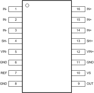
GUID-AC9E6632-3AD6-4528-92E7-DD19FAFB7411-low.gifFigure 5-1 PW Package16-Pin TSSOPTop View
Table 5-1 Pin Functions
PIN I/O DESCRIPTION
NAME NO.
GND 6, 8, 11 Analog Ground
IN– 1, 2, 3 Analog input Connect to load
IN+ 14, 15, 16 Analog input Connect to supply
OUT 9 Analog output Output voltage
REF 7 Analog input Reference voltage, 0 V to VS (up to 18 V)
SH– 4 Analog output Kelvin connection to internal shunt. Connect to VIN– if no filtering is needed.
See Figure 7-4 for filter recommendations.
SH+ 13 Analog output Kelvin connection to internal shunt. Connect to VIN+ if no filtering is needed.
See Figure 7-4 for filter recommendations.
VIN– 5 Analog input Voltage input from load side of shunt resistor.
VIN+ 12 Analog input Voltage input from supply side of shunt resistor.
VS 10 Analog Device power supply, 2.7 V to 36 V