ZHCSIA5A July   2018  – December 2018 INA253

PRODUCTION DATA.  

  1. 特性
  2. 应用
  3. 说明
    1.     典型应用
  4. 修订历史记录
  5. Device Comparison Table
  6. Pin Configuration and Functions
    1.     Pin Functions
  7. Specifications
    1. 7.1 Absolute Maximum Ratings
    2. 7.2 ESD Ratings
    3. 7.3 Recommended Operating Conditions
    4. 7.4 Thermal Information
    5. 7.5 Electrical Characteristics
    6. 7.6 Typical Characteristics
  8. Detailed Description
    1. 8.1 Overview
    2. 8.2 Functional Block Diagram
    3. 8.3 Feature Description
      1. 8.3.1 Integrated Shunt Resistor
      2. 8.3.2 Short-Circuit Duration
      3. 8.3.3 Temperature Stability
      4. 8.3.4 Enhanced PWM Rejection Operation
      5. 8.3.5 Input Signal Bandwidth
    4. 8.4 Device Functional Modes
      1. 8.4.1 Adjusting the Output Midpoint With the Reference Pins
      2. 8.4.2 Reference Pin Connections for Unidirectional Current Measurements
      3. 8.4.3 Ground Referenced Output
      4. 8.4.4 Reference Pin Connections for Bidirectional Current Measurements
        1. 8.4.4.1 Output Set to External Reference Voltage
      5. 8.4.5 Output Set to Mid-Supply Voltage
      6. 8.4.6 Output Set to Mid-External Reference
      7. 8.4.7 Output Set Using Resistor Divide
  9. Application and Implementation
    1. 9.1 Application Information
      1. 9.1.1 Input Filtering
    2. 9.2 Typical Applications
      1. 9.2.1 High-Side, High-Drive, Solenoid Current-Sense Application
        1. 9.2.1.1 Design Requirements
        2. 9.2.1.2 Detailed Design Procedure
        3. 9.2.1.3 Application Curve
      2. 9.2.2 Speaker Enhancements and Diagnostics Using Current Sense Amplifier
        1. 9.2.2.1 Design Requirements
        2. 9.2.2.2 Detailed Design Procedure
        3. 9.2.2.3 Application Curve
      3. 9.2.3 Current Sensing for Remote I/Os in PLC
        1. 9.2.3.1 Design Requirements
        2. 9.2.3.2 Application Curve
  10. 10Power Supply Recommendations
  11. 11Layout
    1. 11.1 Layout Guidelines
    2. 11.2 Layout Example
  12. 12器件和文档支持
    1. 12.1 器件支持
      1. 12.1.1 开发支持
    2. 12.2 相关文档
    3. 12.3 接收文档更新通知
    4. 12.4 社区资源
    5. 12.5 商标
    6. 12.6 静电放电警告
    7. 12.7 术语表
  13. 13机械、封装和可订购信息

封装选项

机械数据 (封装 | 引脚)
散热焊盘机械数据 (封装 | 引脚)
订购信息

Typical Characteristics

at TA = 25°C, VS = 5 V, VIN+ = 12 V, and VREF = VS / 2 (unless otherwise noted)
INA253 D001-SLOS954-01.gif
All gains
Figure 1. Input Offset Voltage Production Distribution
INA253 D003-SLOS954-01.gif
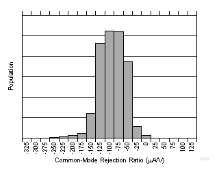
All gains
Figure 3. Common-Mode Rejection Production Distribution
INA253 D005-SLOS954-02.gif
Figure 5. Power-Supply Rejection Ratio vs Temperature
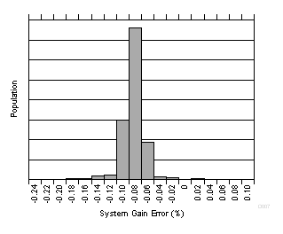
INA253 D007-SLOS954-01.gif
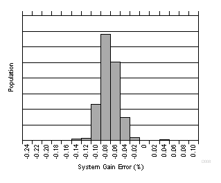
Figure 7. Gain Error Production Distribution (INA253A2)
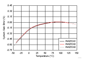
INA253 D009-SLOS954-01.gif
Figure 9. System Gain Error vs Temperature
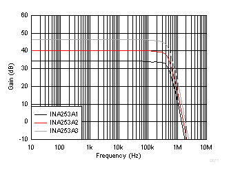
INA253 D011-SLOS954-01.gif
VCM = 0 V, VDIFF = 10-mVPP sine
Figure 11. Amplifier Gain Error vs Frequency
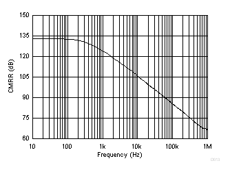
INA253 D013-SLOS954-01.gif
Figure 13. Common-Mode Rejection Ratio vs Frequency
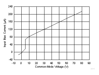
INA253 D015-SLOS954-01.gif
VS = 5 V
Figure 15. Input Bias Current vs Common-Mode Voltage
INA253 D017-SLOS954-01.gif
Figure 17. Input Bias Current vs Temperature
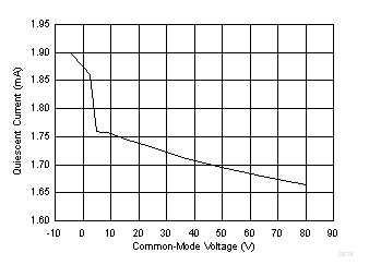
INA253 D019-SLOS954-01.gif
Figure 19. Quiescent Current vs Common-mode Voltage
INA253 D021-SLOS954-01.gif
Figure 21. INA253A2 Input-Referred Voltage Noise vs Frequency
INA253 D023-SLOS954-01.gif
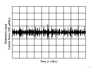
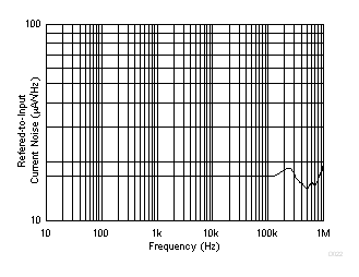
Figure 23. 0.1-Hz to 10-Hz Voltage Noise (Referred-to-Input)
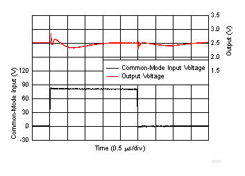
INA253 D025-SLOS954-01.gif
VREF1 = VREF2 = 0 V
Figure 25. Common-Mode Transient Response
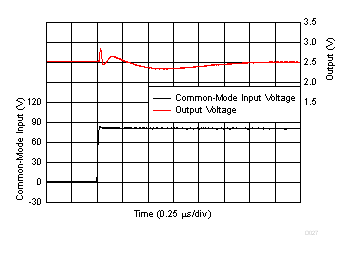
INA253 D027-SLOS954-01.gif
Rising Edge
Figure 27. Common-Mode Voltage Transient Response
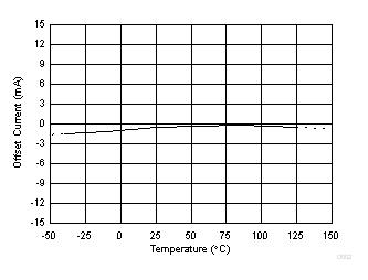
INA253 D002-SLOS954-01.gif
Figure 2. Input Offset Current vs Temperature
INA253 D004-SLOS954-01.gif
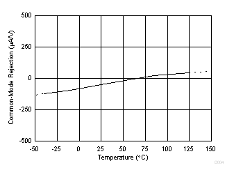
Figure 4. Common-Mode Rejection Ratio vs Temperature
INA253 D006-SLOS954-01.gif
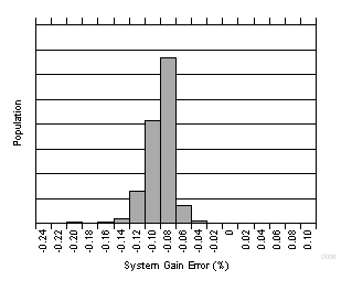
Figure 6. Gain Error Production Distribution (INA253A1)
INA253 D008-SLOS954-01.gif
Figure 8. Gain Error Production Distribution (INA253A3)
INA253 D010-SLOS954-01.gif
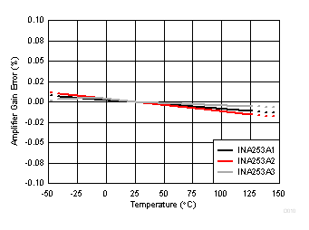
Figure 10. Amplifier Gain Error vs Temperature
INA253 D012-SLOS954-01.gif
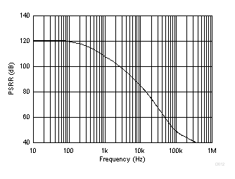
Figure 12. Power-Supply Rejection Ratio vs Frequency
INA253 D014-SLOS954-01.gif
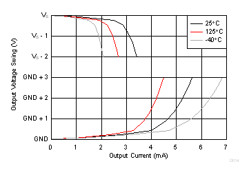
VS = 5 V
Figure 14. Output Voltage Swing vs Output Current
INA253 D016-SLOS954-01.gif
VS = 0 V
Figure 16. Input Bias Current vs Common-Mode Voltage
INA253 D018-SLOS954-02.gif
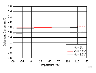
Figure 18. Quiescent Current vs Temperature
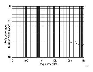
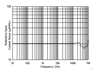
INA253 D020-SLOS954-01.gif
Figure 20. INA253A1 Input-Referred Voltage Noise vs Frequency
INA253 D022-SLOS954-01.gif
Figure 22. INA253A3 Input-Referred Voltage Noise vs Frequency
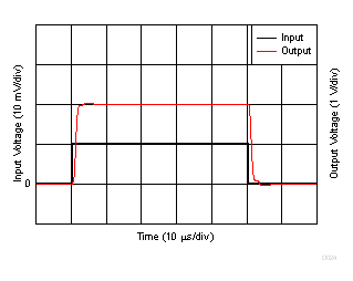
INA253 D024-SLOS954-01.gif
VREF1 = VREF2 = 0 V, 10-mVPP input step
Figure 24. Amplifier Step Response
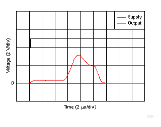
INA253 D026-SLOS954-01.gif
Figure 26. Start-Up Response
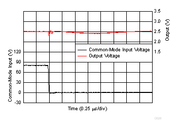
INA253 D028-SLOS954-01.gif
Falling Edge
Figure 28. Common-Mode Voltage Transient Response