ZHCSO13A june 2021 – march 2023 INA254
PRODUCTION DATA
- 1 特性
- 2 应用
- 3 说明
- 4 Revision History
- 5 Device Comparison
- 6 Pin Configuration and Functions
- 7 规格
-
8 Detailed Description
- 8.1 Overview
- 8.2 Functional Block Diagram
- 8.3 Feature Description
- 8.4
Device Functional Modes
- 8.4.1 Adjusting the Output Midpoint With the Reference Pins
- 8.4.2 Reference Pin Connections for Unidirectional Current Measurements
- 8.4.3 Ground Referenced Output
- 8.4.4 Reference Pin Connections for Bidirectional Current Measurements
- 8.4.5 Output Set to Mid-Supply Voltage
- 8.4.6 Output Set to Mid-External Reference
- 8.4.7 Output Set Using Resistor Divider
- 9 Application and Implementation
- 10Device and Documentation Support
- 11Mechanical, Packaging, and Orderable Information
8.3.5 Input Signal Bandwidth
The INA254 input signal, which represents the current being measured, is accurately measured with minimal disturbance from large ΔV/Δt common-mode transients as previously described. For PWM signals typically associated with motors, solenoids, and other switching applications, the current being monitored varies at a significantly slower rate than the faster PWM frequency.
The INA254 bandwidth is defined by the –3-dB bandwidth of the current-sense amplifier inside the device. The device bandwidth provides fast throughput and fast response required for the rapid detection and processing of overcurrent events. Without the higher bandwidth, protection circuitry may not have adequate response time, and damage may occur to the monitored application or circuit.
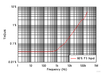
Figure 8-4 shows the performance profile of the device over frequency. Harmonic distortion increases at the upper end of the amplifier bandwidth with no adverse change in detection of overcurrent events. However, increased distortion at the highest frequencies must be considered when the measured current bandwidth begins to approach the INA254 bandwidth.
 Figure 8-4 Amplifier Performance Over Frequency
For applications requiring distortion sensitive signals, Figure 8-4 provides information to show that there is an optimal frequency performance range for the amplifier. The full amplifier bandwidth is always available for fast overcurrent events at the same time that the lower-frequency signals are amplified at a low distortion level. The output signal accuracy is reduced for frequencies closer to the maximum bandwidth. Individual requirements determine the acceptable limits of distortion for high-frequency, current-sensing applications. Testing and evaluation in the end application or circuit are required to determine the acceptance criteria, and to validate the performance levels meet the system specifications.