SBOS401C July 2007 – April 2016 INA270A-Q1 , INA271A-Q1
PRODUCTION DATA.
- 1 Features
- 2 Applications
- 3 Description
- 4 Revision History
- 5 Device Comparison Table
- 6 Pin Configuration and Functions
- 7 Specifications
- 8 Detailed Description
- 9 Application and Implementation
- 10Power Supply Recommendations
- 11Layout
- 12Device and Documentation Support
- 13Mechanical, Packaging, and Orderable Information
9 Application and Implementation
NOTE
Information in the following applications sections is not part of the TI component specification, and TI does not warrant its accuracy or completeness. TI’s customers are responsible for determining suitability of components for their purposes. Customers should validate and test their design implementation to confirm system functionality.
9.1 Application Information
The INA27xA-Q1 measures the voltage developed across a current-sensing resistor when current passes through it. There is also a filtering feature to remove unwanted transients and smooth the output voltage.
9.1.1 Basic Connection
Figure 16 illustrates the basic connection of the INA27xA-Q1. The input pins, IN+ and IN–, should be connected as closely as possible to the shunt resistor to minimize any resistance in series with the shunt resistance. Power-supply bypass capacitors are required for stability. Applications with noisy or high-impedance power supplies may require additional decoupling capacitors to reject power-supply noise. Minimum bypass capacitors of 0.01 μF and 0.1 μF in value should be placed close to the supply pins. Although not mandatory, an additional 10-µF electrolytic capacitor placed in parallel with the other bypass capacitors may be useful in applications with particularly noisy supplies.
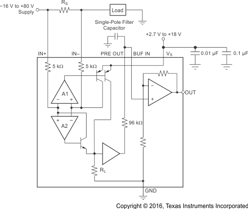 Figure 16. INA270A-Q1 Basic Connection
9.1.2 Selecting RS
The value chosen for the shunt resistor, RS, depends on the application and is a compromise between small-signal accuracy and maximum permissible voltage loss in the measurement line. High values of RS provide better accuracy at lower currents by minimizing the effects of offset, while low values of RS minimize voltage loss in the supply line. For most applications, best performance is attained with an RS value that provides a full-scale shunt voltage range of 50 mV to 100 mV. Maximum input voltage for accurate measurements is (VS – 0.2)/Gain.
9.1.3 Accuracy Variations as a Result of VSENSE and Common-Mode Voltage
The accuracy of the INA27xA-Q1 current-shunt monitors is a function of two main variables: VSENSE (VIN+ – VIN–) and common-mode voltage, VCM, relative to the supply voltage, VS. VCM is expressed as (VIN+ + VIN–)/2; however, in practice, VCM is seen as the voltage at VIN+ because the voltage drop across VSENSE is usually small.
This section addresses the accuracy of these specific operating regions:
Normal Case 1: VSENSE ≥ 20 mV, VCM ≥ VS
Normal Case 2: VSENSE ≥ 20 mV, VCM < VS
Low VSENSE Case 1: VSENSE < 20 mV, –16 V ≤ VCM < 0
Low VSENSE Case 2: VSENSE < 20 mV, 0 V ≤ VCM ≤ VS
Low VSENSE Case 3: VSENSE < 20 mV, VS < VCM ≤ 80 V
9.1.3.1 Normal Case 1: VSENSE ≥ 20 mV, VCM ≥ VS
This region of operation provides the highest accuracy. Here, the input offset voltage is characterized and measured using a two-step method. First, the gain is determined by Equation 1.

where
- VOUT1 = Output voltage with VSENSE = 100 mV
- VOUT2 = Output voltage with VSENSE = 20 mV
Then the offset voltage is measured at VSENSE = 100 mV and referred to the input (RTI) of the current-shunt monitor, as shown in Equation 2.

In Typical Characteristics, the Output Error vs Common-Mode Voltage curve shows the highest accuracy for the this region of operation. In this plot, VS = 12 V; for VCM ≥ 12 V, the output error is at its minimum. This case is also used to create the VSENSE ≥ 20 mV output specifications in Electrical Characteristics.
9.1.3.2 Low VSENSE Case 1: VSENSE < 20 mV, –16 V ≤ VCM < 0; and
Low VSENSE Case 3: VSENSE < 20 mV, VS < VCM ≤ 80 V
Although the INA270A-Q1 family of devices are not designed for accurate operation in either of these regions, some applications are exposed to these conditions. For example, when monitoring power supplies that are switched on and off while VS is still applied to the INA27xA-Q1 devices, it is important to know what the behavior of the devices is in these regions.
As VSENSE approaches 0 mV, in these VCM regions, the device output accuracy degrades. A larger-than-normal offset can appear at the current-shunt monitor output with a typical maximum value of VOUT = 60 mV for VSENSE = 0 mV. As VSENSE approaches 20 mV, VOUT returns to the expected output value with accuracy as specified in Electrical Characteristics. Figure 17 illustrates this effect using the INA271A-Q1 (Gain = 20).
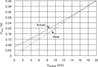 Figure 17. Example for Low VSENSE Cases 1 and 3 (INA271A-Q1, Gain = 20)
9.1.3.3 Low VSENSE Case 2: VSENSE < 20 mV, 0 V ≤ VCM ≤ VS
This region of operation is the least accurate for the INA27xA-Q1 family. To achieve the wide input common-mode voltage range, these devices use two operational amplifier (op amp) front ends in parallel. One op amp front end operates in the positive input common-mode voltage range, and the other in the negative input region. For this case, neither of these two internal amplifiers dominates and overall loop gain is very low. Within this region, VOUT approaches voltages close to linear operation levels for Normal Case 2.
This deviation from linear operation becomes greatest the closer VSENSE approaches 0 V. Within this region, as VSENSE approaches 20 mV, device operation is closer to that described by Normal Case 2. Figure 18 illustrates this behavior for the INA271A-Q1. The VOUT maximum peak for this case is determined by maintaining a constant VS, setting VSENSE = 0 mV and sweeping VCM from 0 V to VS. The exact VCM at which VOUT peaks during this case varies from part to part. The maximum peak voltage for the INA270A-Q1 is 0.28 V; for the INA271A-Q1, the maximum peak voltage is 0.4 V.
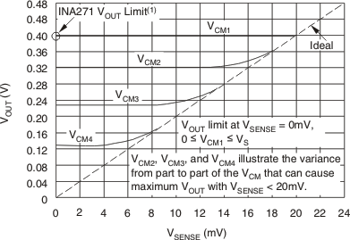 Figure 18. Example for Low VSENSE Case 2 (INA271A-Q1, Gain = 20)
9.1.4 Transient Protection
The –16-V to 80-V common-mode range of the INA27xA-Q1 is ideal for withstanding automotive fault conditions ranging from 12-V battery reversal up to 80-V transients, since no additional protective components are needed up to those levels. In the event that the INA27xA-Q1 devices are exposed to transients on the inputs in excess of their ratings, external transient absorption with semiconductor transient absorbers (zeners or Transzorbs) are necessary.
Use of MOVs or VDRs is not recommended except when they are used in addition to a semiconductor transient absorber. Select the transient absorber such that it never allows the INA27xA-Q1 to be exposed to transients greater than 80 V (that is, allow for transient absorber tolerance, as well as additional voltage because of transient absorber dynamic impedance).
Despite the use of internal zener-type ESD protection, the INA27xA-Q1 devices are not suited to using external resistors in series with the inputs, since the internal gain resistors can vary up to ±30%, but the internal resistors are tightly matched. If gain accuracy is not important, then resistors can be added in series with the INA27xA-Q1 inputs, with two equal resistors on each input.
9.2 Typical Application
 Figure 19. Filtering Configuration
9.2.1 Design Requirements
In this application, the device is configured to measure a triangular periodic current at 10 kHz with filtering. The average current through the shunt is the information that is desired. This current can be either solenoid current or inductor current where current is being pulsed through.
Selecting the capacitor size is based on the lowest frequency component to be filtered out. The amount of signal that is filtered out is dependant on this cutoff frequency. From the cutoff frequency, the attention is 20 dB per decade.
9.2.2 Detailed Design Procedure
Without this filtering capability, an input filter must be used. When series resistance is added to the input, large errors also come into play because the resistance must be large to create a low cutoff frequency. By using a
10-nF capacitor for the single-pole filter capacitor, the 10-kHz signal is averaged. The cutoff frequency made by the capacitor is set at 166 Hz frequency. This frequency is well below the periodic frequency and reduces the ripple on the output and the average current can easily be measured.
9.2.3 Application Curves
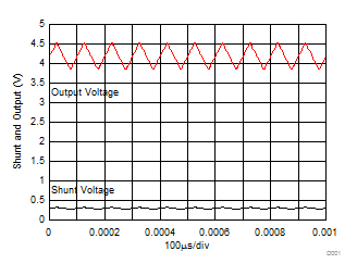
Figure 20 shows the output waveform without filtering. The output signal tracks the input signal with a large ripple. If this current is sampled by an ADC, many samples must be taken to average the current digitally. This process takes additional time to sample and average and is very time consuming, thus is unwanted for this application.
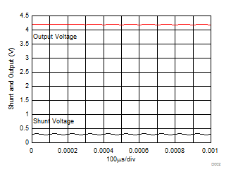
Figure 21 shows the output waveform with filtering. The output signal is filtered and the average can easily be measured with a small ripple. If this current is sampled by an ADC, only a few samples must be taken to average. Digital averaging is now not required and the time required is significantly reduced.
