SBOS401C July 2007 – April 2016 INA270A-Q1 , INA271A-Q1
PRODUCTION DATA.
- 1 Features
- 2 Applications
- 3 Description
- 4 Revision History
- 5 Device Comparison Table
- 6 Pin Configuration and Functions
- 7 Specifications
- 8 Detailed Description
- 9 Application and Implementation
- 10Power Supply Recommendations
- 11Layout
- 12Device and Documentation Support
- 13Mechanical, Packaging, and Orderable Information
11 Layout
11.1 Layout Guidelines
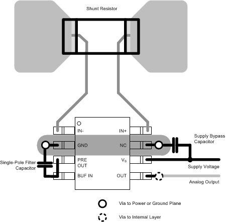
- Connect the input pins to the sensing resistor using a Kelvin or 4-wire connection. This connection technique ensures that only the current-sensing resistor impedance is detected between the input pins. Poor routing of the current-sensing resistor commonly results in additional resistance present between the input pins. Given the very low ohmic value of the current resistor, any additional high-current carrying impedance can cause significant measurement errors.
- Place the power-supply bypass capacitor as closely as possible to the supply and ground pins. The recommended value of this bypass capacitor is 0.1 μF. Additional decoupling capacitance can be added to compensate for noisy or high-impedance power supplies.
11.1.1 RFI and EMI
Attention to good layout practices is always recommended. Keep traces short and, when possible, use a printed circuit board (PCB) ground plane with surface-mount components placed as close to the device pins as possible. Small ceramic capacitors placed directly across amplifier inputs can reduce RFI and EMI sensitivity. PCB layout should locate the amplifier as far away as possible from RFI sources. Sources can include other components in the same system as the amplifier itself, such as inductors (particularly switched inductors handling a lot of current and at high frequencies). RFI can generally be identified as a variation in offset voltage or dc signal levels with changes in the interfering RF signal. If the amplifier cannot be located away from sources of radiation, shielding may be needed. Twisting wire input leads makes them more resistant to RF fields. The difference in input pin location of the INA27xA-Q1 versus the INA193 through INA198 may provide different EMI performance.
11.2 Layout Example
 Figure 23. INA27xA-Q1 Example Layout