SBOS401C July 2007 – April 2016 INA270A-Q1 , INA271A-Q1
PRODUCTION DATA.
- 1 Features
- 2 Applications
- 3 Description
- 4 Revision History
- 5 Device Comparison Table
- 6 Pin Configuration and Functions
- 7 Specifications
- 8 Detailed Description
- 9 Application and Implementation
- 10Power Supply Recommendations
- 11Layout
- 12Device and Documentation Support
- 13Mechanical, Packaging, and Orderable Information
7 Specifications
7.1 Absolute Maximum Ratings
over operating free-air temperature range (unless otherwise noted)(1)
(1) Stresses beyond those listed under Absolute Maximum Ratings may cause permanent damage to the device. These are stress ratings only, which do not imply functional operation of the device at these or any other conditions beyond those indicated under Recommended Operating Conditions. Exposure to absolute-maximum-rated conditions for extended periods may affect device reliability.
7.2 ESD Ratings
| VALUE | UNIT | |||
|---|---|---|---|---|
| V(ESD) | Electrostatic discharge | Human-body model (HBM), per AEC Q100-002(1) | 2000 | V |
| Machine Model (MM) | 100 | |||
| Charged-device model (CDM), per AEC Q100-011 | 1000 | |||
(1) AEC Q100-002 indicates that HBM stressing shall be in accordance with the ANSI/ESDA/JEDEC JS-001 specification.
7.3 Recommended Operating Conditions
| MIN | NOM | MAX | UNIT | |||
|---|---|---|---|---|---|---|
| VS | Supply voltage | 2.7 | 5 | 18 | V | |
| VCM | Common mode input | –16 | 12 | 80 | V | |
| TA | Operating free-air temperature | –40 | 25 | 125 | °C | |
7.4 Thermal Information
| THERMAL METRIC(1) | INA27xA-Q1 | UNIT | |
|---|---|---|---|
| D (SOIC) | |||
| 8 PINS | |||
| RθJA | Junction-to-ambient thermal resistance | 78.8 | °C/W |
| RθJC(top) | Junction-to-case (top) thermal resistance | 71.6 | °C/W |
| RθJB | Junction-to-board thermal resistance | 68.2 | °C/W |
| ψJT | Junction-to-top characterization parameter | 22 | °C/W |
| ψJB | Junction-to-board characterization parameter | 67.6 | °C/W |
| RθJC(bot) | Junction-to-case (bottom) thermal resistance | n/a | °C/W |
(1) For more information about traditional and new thermal metrics, see the Semiconductor and IC Package Thermal Metrics application report, SPRA953.
7.5 Electrical Characteristics
TA = 25°C, VS = 5 V, VCM = 12 V, VSENSE = 100 mV, PRE OUT connected to BUF IN (unless otherwise noted)| PARAMETER | TEST CONDITIONS | MIN | TYP | MAX | UNIT | ||
|---|---|---|---|---|---|---|---|
| Input | |||||||
| VSENSE | Full-scale input voltage | VSENSE = VIN+ - VIN– | 0.15 | (VS – 0.2)/ Gain | V | ||
| VCM | Common-mode input voltage | TA = –40°C to +125°C | –16 | 80 | V | ||
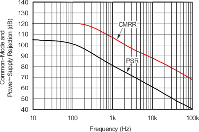
| CMRR | Common-mode rejection | VIN+ = –16 V to +80 V | 80 | 120 | dB | ||
| VIN+ = 12 V to 80 V, TA = –40°C to +125°C |
100 | 120 | |||||
| VOS | Offset voltage, RTI(1) | ±0.5 | 2.5 | mV | |||
| TA = –40°C to +125°C | ±3 | ||||||
| dVOS/dT | Input offset voltage temperature coefficient | TA = –40°C to +125°C | 2.5 | 20 | μV/°C | ||
| PSR | Offset voltage power-supply rejection | VS = 2.7 V to 18 V, VCM = 18 V, TA = –40°C to +125°C | 5 | 100 | μV/V | ||
| IIB | Input bias current | IN– pin, TA = –40°C to +125°C full range | ±8 | ±16 | μA | ||
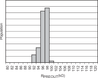
| ZO | Output impedance(2) | PRE OUT pin | 96 | kΩ | |||
| Buffer input bias current | –50 | nA | |||||
| Buffer input bias current temperature coefficient | ±0.3 | nA/°C | |||||
| Output (VSENSE ≥ 20 mV)(3) | |||||||
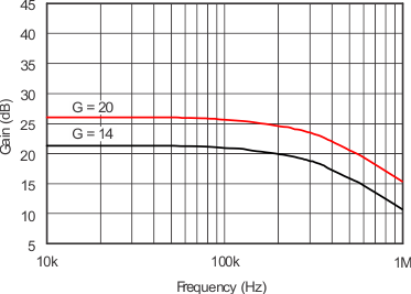
| G | Gain | INA270A-Q1 | 14 | V/V | |||
| INA271A-Q1 | 20 | ||||||
| GBUF | Output buffer gain | 2 | V/V | ||||
| Total gain error | VSENSE = 20 mV to 100 mV | ±0.2% | ±1% | ||||
| TA = –40°C to +125°C | ±2% | ||||||
| Total gain error temperature coefficient | TA = –40°C to +125°C | 50 | ppm/°C | ||||
| Total output error(4) | ±0.75% | ±2.2% | |||||
| TA = –40°C to +125°C | ±1% | ±3% | |||||
| Nonlinearity error | VSENSE = 20 mV to 100 mV | ±0.002% | |||||
| ZO | Output impedance | OUT pin | 1.5 | Ω | |||
| Maximum capacitive load | No sustained oscillation | 10 | nF | ||||
| Voltage Output(5) | |||||||
| Swing to VS power-supply rail | RL = 10 kΩ to GND, TA = –40°C to +125°C | VS – 0.05 | VS – 0.2 | V | |||
| Swing to GND | RL = 10 kΩ to GND, TA = –40°C to +125°C | VGND + 0.003 | VGND + 0.05 | V | |||
| Frequency Response | |||||||
| BW | Bandwidth | CL = 5 pF | 130 | kHz | |||
| φm | Phase margin | CL < 10 nF | 40 | degrees | |||
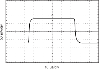
| SR | Slew rate | 1 | V/μs | ||||
| ts | Settling time (1%) | VSENSE = 10 mV to 100 mV, CL = 5 pF | 2 | μs | |||
| Noise, RTI(1) | |||||||
| Vn | Voltage noise density | 40 | nV/√Hz | ||||
| Power Supply | |||||||
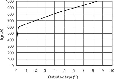
| IQ | Quiescent current | VOUT = 2 V | 700 | 900 | μA | ||
| VSENSE = 0 V, TA = –40°C to +125°C | 350 | 950 | |||||
(1) RTI = referred to input
(2) Initial resistor variation is ±30% with an additional –2200-ppm/°C temperature coefficient.
(3) For output behavior when VSENSE < 20 mV, see Application Information
(4) Total output error includes effects of gain error and VOS.
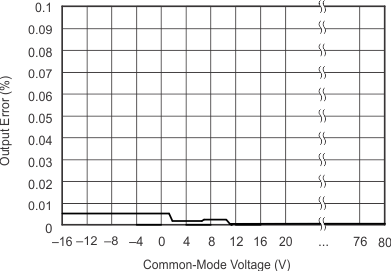
(5) See Typical Characteristics curve Output Swing vs Output Current and Accuracy Variations as a Result of VSENSE and Common-Mode Voltage in the Application Information section.
7.6 Typical Characteristics
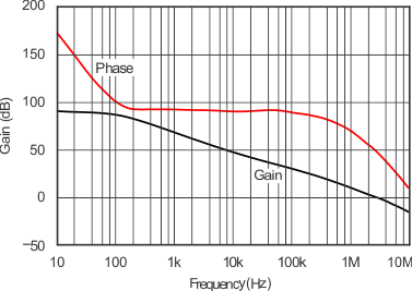
TA = 25°C, VS = 12 V, VCM = 12 V, VSENSE = 100 mV (unless otherwise noted)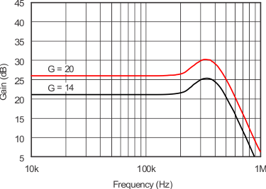
| CLOAD = 1000 pF |

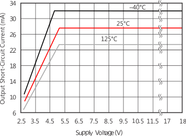
| VS = 18 V |
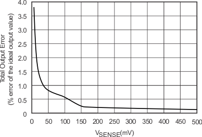
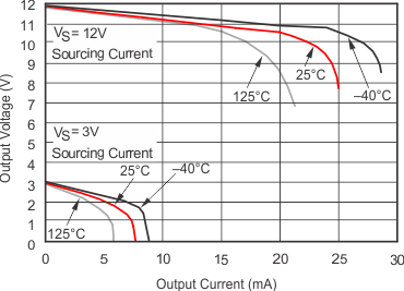
| Output stage is designed to source current. | ||
| Current sinking capability is approximately 400 μA. | ||

| CLOAD = 0 pF |
