SBOS485C November 2009 – May 2015 INA282 , INA283 , INA284 , INA285 , INA286
PRODUCTION DATA.
- 1 Features
- 2 Applications
- 3 Description
- 4 Revision History
- 5 Pin Configuration and Functions
- 6 Specifications
- 7 Detailed Description
- 8 Applications and Implementation
- 9 Power Supply Recommendations
- 10Layout
- 11Device and Documentation Support
- 12Mechanical, Packaging, and Orderable Information
8 Applications and Implementation
NOTE
Information in the following applications sections is not part of the TI component specification, and TI does not warrant its accuracy or completeness. TI’s customers are responsible for determining suitability of components for their purposes. Customers should validate and test their design implementation to confirm system functionality.
8.1 Application Information
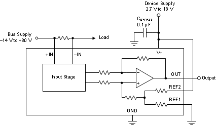
The INA28x family of devices measure the voltage developed across a current-sensing resistor when current passes through it. The ability to drive the reference pins to adjust the functionality of the output signal is shown in multiple configurations.
8.1.1 Basic Connections
Figure 39 shows the basic connection of an INA28x family device. Connect the input pins, +IN and –IN, as closely as possible to the shunt resistor to minimize any resistance in series with the shunt resistance.
Power-supply bypass capacitors are required for stability. Applications with noisy or high-impedance power supplies may require additional decoupling capacitors to reject power-supply noise. Connect bypass capacitors close to the device pins.
8.2 Typical Applications
8.2.1 Current Summing
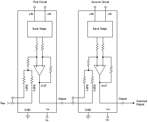
The outputs of multiple INA28x family devices are easily summed by connecting the output of one INA28x family device to the reference input of a second INA28x family device. The circuit configuration shown in Figure 40 is an easy way to achieve current summing.
8.2.1.1 Design Requirements
In order to sum multiple load currents, multiple INA28x devices must be connected. Figure 40 shows summing for two devices. Summing beyond two devices is possible by repeating this connection. The reference input of the first INA28x family device sets the output quiescent level for all the devices in the string.
8.2.1.2 Detailed Design Procedure
Connect the output of one INA28x family device to the reference input of the next INA28x family device in the chain. Use the reference input of the first circuit to set the reference of the final summed output. The currents sensed at each circuit in the chain are summed at the output of the last device in the chain.
8.2.1.3 Application Curves
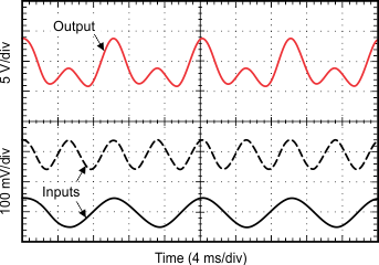
An example output response of a summing configuration is shown in Figure 41. The reference pins of the first circuit are connected to ground, and sine waves at different frequencies are applied to the two circuits to produce a summed output as shown. The sine wave voltage input for the first circuit is offset so that the whole wave is above GND.
| VREF = 0 V | ||
8.2.2 Current Differencing
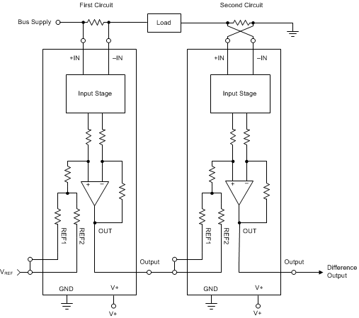
Occasionally, the need arises to confirm that the current into a load is identical to the current out of a load, usually as part of diagnostic testing or fault detection. This situation requires precision current differencing, which is the same as summing except that the two amplifiers have the inputs connected opposite of each other.
8.2.2.1 Design Requirements
For current differencing, connect two INA28x devices, and have the inputs connected opposite to each other, as shown in Figure 42. The reference input of the first INA28x family device sets the output quiescent level for all the devices in the string.
8.2.2.2 Detailed Design Procedure
Connect the output of one INA28x family device to the reference input of the second INA28x family device. The reference input of the first circuit sets the reference at the output. This circuit example is identical to the current summing example, except that the two shunt inputs are reversed in polarity. Under normal operating conditions, the final output is very close to the reference value and proportional to any current difference. This current differencing circuit is useful in detecting when current in to and out of a load do not match.
8.2.2.3 Application Curves
An example output response of a difference configuration is shown in Figure 43. The reference pins of the first circuit are connected to a reference voltage of 2.048 V. The inputs to each circuit is a 100-Hz sine wave, 180° out of phase with each other, resulting in a zero output as shown. The sine wave input to the first circuit is offset so that the input wave is completely above GND.
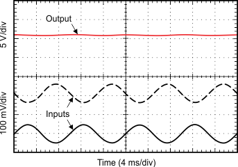
| VREF = 2.048 V | ||
