ZHCSEX8B December 2015 – December 2021 INA300-Q1
PRODUCTION DATA
- 1 特性
- 2 应用
- 3 说明
- 4 Revision History
- 5 Pin Configuration and Functions
- 6 Specifications
-
7 Detailed Description
- 7.1 Overview
- 7.2 Functional Block Diagram
- 7.3 Feature Description
- 7.4 Device Functional Modes
- 8 Application and Implementation
- 9 Power Supply Recommendations
- 10Layout
- 11Device and Documentation Support
- 12Mechanical, Packaging, and Orderable Information
6.7 Typical Characteristics
at TA = 25°C, VS = 3.3 V, VIN+ = 12 V, alert pull-up resistor = 10 kΩ, and Delay = 100 µs (unless otherwise noted)
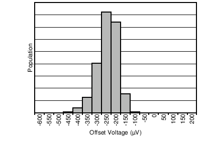
| Delay = 10 µs |
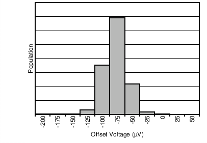
| Delay = 100 µs |
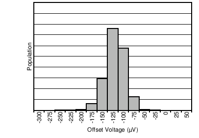
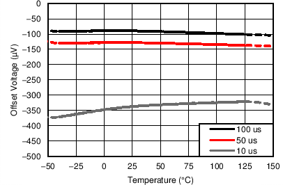 Figure 6-5 Input Offset Voltage vs.
Temperature
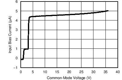 Figure 6-7 Input Bias Current vs.
Common-Mode Voltage (Enabled)
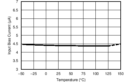 Figure 6-9 Input Bias Current vs.
Temperature (Enabled)
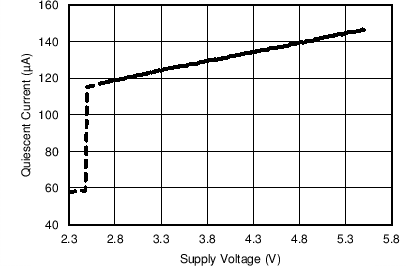 Figure 6-11 Quiescent Current vs.
Supply Voltage (Enabled)
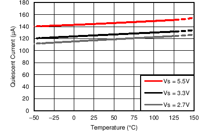 Figure 6-13 Quiescent Current vs.
Temperature (Enabled)
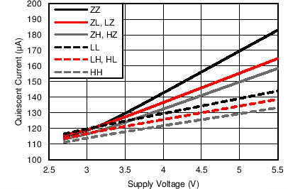
| Z = Floating | L = Low | H = High |
| HYS – DELAY |
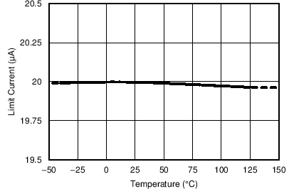 Figure 6-17 Limit Current Source vs.
Temperature
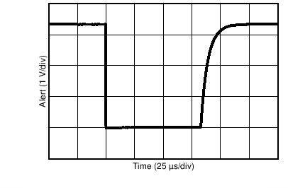 Figure 6-19 Alert Step Response
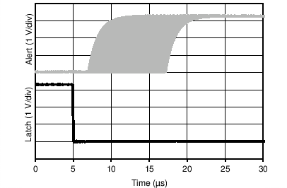 Figure 6-21 Alert Response (Latch Mode to Transparent Mode)
| Delay = 50 µs |
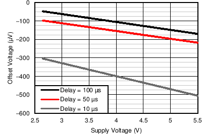
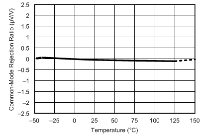 Figure 6-6 Common-Mode Rejection
Ratio vs. Temperature
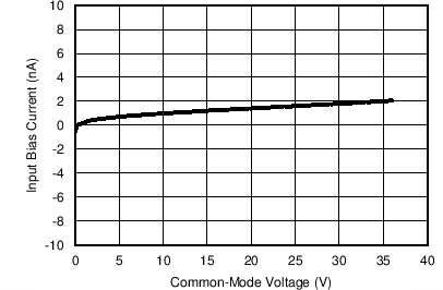 Figure 6-8 Input Bias Current vs.
Common-Mode Voltage (Disabled)
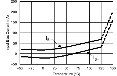 Figure 6-10 Input Bias Current vs.
Temperature (Disabled)
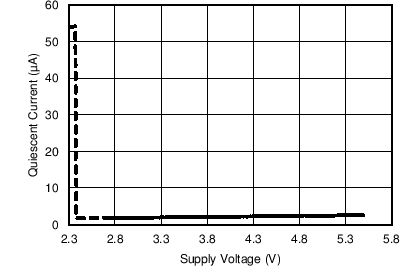 Figure 6-12 Quiescent Current vs.
Supply Voltage (Disabled)
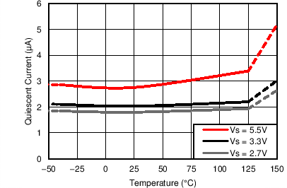 Figure 6-14 Quiescent Current vs.
Temperature (Disabled)
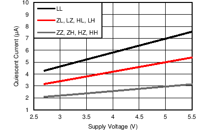
| Z = Floating | L = Low | H = High |
| HYS – DELAY |
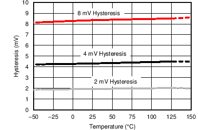 Figure 6-18 Hysteresis vs.
Temperature
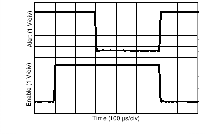 Figure 6-20 Alert Response (Disable to Enable)