ZHCSC46C February   2014  – June 2021 INA300

PRODUCTION DATA  

  1. 特性
  2. 应用
  3. 说明
  4. Revision History
  5. Pin Configuration and Functions
  6. Specifications
    1. 6.1 Absolute Maximum Ratings (1)
    2. 6.2 ESD Ratings
    3. 6.3 Recommended Operating Conditions
    4. 6.4 Thermal Information
    5. 6.5 Electrical Characteristics
    6. 6.6 Timing Requirements
    7. 6.7 Typical Characteristics
  7. Detailed Description
    1. 7.1 Overview
    2. 7.2 Functional Block Diagram
    3. 7.3 Feature Description
      1. 7.3.1 Selecting a Current-Sensing Resistor
        1. 7.3.1.1 Selecting a Current-Sensing Resistor: Example
      2. 7.3.2 Setting The Current-Limit Threshold
        1. 7.3.2.1 Resistor-Controlled Current Limit
        2. 7.3.2.2 Voltage Source-Controlled Current Limit
      3. 7.3.3 Delay Setting
      4. 7.3.4 Alert Timing Response
      5. 7.3.5 Selectable Hysteresis
      6. 7.3.6 Alert Output
      7. 7.3.7 Noise Adjustment Factor (NAF)
    4. 7.4 Device Functional Modes
      1. 7.4.1 Alert Mode
        1. 7.4.1.1 Transparent Output Mode
        2. 7.4.1.2 Latch Output Mode
      2. 7.4.2 Disable Mode
      3. 7.4.3 Input Filtering
      4. 7.4.4 Using the INA300 INA300 With Common-Mode Transients Above 36 V
  8. Application and Implementation
    1. 8.1 Application Information
    2. 8.2 Typical Applications
      1. 8.2.1 Unidirectional Operation
        1. 8.2.1.1 Design Requirements
        2. 8.2.1.2 Detailed Design Procedure
        3. 8.2.1.3 Application Curve
      2. 8.2.2 Bidirectional Operation
        1. 8.2.2.1 Design Requirements
        2. 8.2.2.2 Detailed Design Procedure
        3. 8.2.2.3 Application Curve
      3. 8.2.3 Window Comparator
        1. 8.2.3.1 Design Requirements
        2. 8.2.3.2 Detailed Design Procedure
        3. 8.2.3.3 Application Curve
  9. Power Supply Recommendations
  10. 10Layout
    1. 10.1 Layout Guidelines
    2. 10.2 Layout Example
  11. 11Device and Documentation Support
    1. 11.1 Documentation Support
      1. 11.1.1 Related Documentation
    2. 11.2 接收文档更新通知
    3. 11.3 支持资源
    4. 11.4 Trademarks
    5. 11.5 Electrostatic Discharge Caution
    6. 11.6 术语表
  12. 12Mechanical, Packaging, and Orderable Information

封装选项

机械数据 (封装 | 引脚)
散热焊盘机械数据 (封装 | 引脚)
订购信息

Application Curve

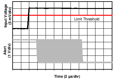
Figure 8-2 shows the alert response transitioning from a high to a low state following the input signal exceeding the limit threshold voltage. The time required for the output to respond varies as a result of when the input signal crosses the threshold limit voltage relative to where in the continuous running internal 10-µs comparison window the overrange condition occurs. In Figure 8-2, the output response varies from roughly 2 µs to approximately
12 µs when the input exceeds the threshold level. This variance is a result of where in the 10-µs comparison window the overrange event occurs. If the overrange event occurs late in the 10-µs comparison window and is large enough to average the entire window measurement up above the threshold level, the alert appears to respond very quickly. If the alert occurs late in the 10-µs comparison window and is not large enough to average the entire window measurement up above the threshold level, the alert does not appear until the next 10-µs comparison window completes, assuming the input signal remains above the threshold for the entire duration.
GUID-B4565384-681C-4309-A296-53D8B710797E-low.pngFigure 8-2 Alert Response