ZHCSC46C February 2014 – June 2021 INA300
PRODUCTION DATA
- 1 特性
- 2 应用
- 3 说明
- 4 Revision History
- 5 Pin Configuration and Functions
- 6 Specifications
-
7 Detailed Description
- 7.1 Overview
- 7.2 Functional Block Diagram
- 7.3 Feature Description
- 7.4 Device Functional Modes
- 8 Application and Implementation
- 9 Power Supply Recommendations
- 10Layout
- 11Device and Documentation Support
- 12Mechanical, Packaging, and Orderable Information
7.3.3 Delay Setting
The device response time for overcurrent events is adjustable based on the DELAY terminal setting. Three response time settings are available, ranging from 10 µs to 100 µs. The primary purpose for the three different delay settings is to offer a trade-off between a faster alert response and a more precise overcurrent threshold level detection.
The device has a 10-µs internal comparison window. This single comparison window is the fundamental time unit used for all three delay settings. For the 10-µs delay setting, the device compares the average of the input signal during the 10-µs comparison window to the threshold limit programmed at the LIMIT terminal. If the averaged input signal exceeds the threshold at the end of the 10-µs comparison window, the output alert triggers and pulls the ALERT terminal low. However, if the averaged input does not exceed the threshold at the end of the 10-µs comparison window, there is no change in the output alert status, which remains high to indicate that no overcurrent event is detected.
For the 50-µs delay setting, there must be five consecutive 10-µs comparison windows that result in an average input signal exceeding the threshold limit in order for the output alert to trigger and pull the ALERT terminal low. If any single 10-µs comparison window fails to detect an overcurrent condition before reaching five consecutive overcurrent comparisons, the internal counter is reset and no output alert is issued. With the internal counter reset, a new group of five consecutive 10-µs comparison windows of overcurrent conditions are required in order to trigger the alert and pull the ALERT terminal low.
The 100-µs delay setting operates in the same manner as the 50-µs method, but instead requires ten consecutive 10-µs comparison windows with an input signal exceeding the threshold limit to issue an output alert and pull the ALERT terminal low.
Requiring multiple consecutive overcurrent detections aides significantly in reducing the likelihood of system noise causing false alerts, which can be detrimental to critical system operations. However, by enabling an alert window equal to the comparison window of 10 µs, the device still has the flexibility to be used in fast overcurrent detection applications that require quick responses to rapidly changing system operating characteristics.
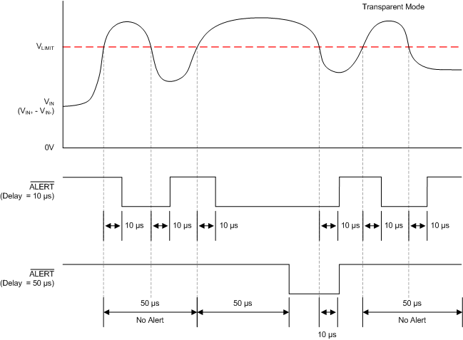
In Figure 7-1, the device alert output response is shown for a 10-µs delay setting and a 50-µs delay setting based on the same input signal condition. The initial increase of the input signal, VIN, above the VLIMIT level remains above the limit for approximately 30 µs. With the device set to the 10-µs delay setting, the overcurrent condition is detected and the alert output terminal is pulled low approximately 10 µs later. With the device set to the 50-µs delay setting, an alert is not issued because five consecutive 10-µs overcurrent measurements are not detected. With the input signal only being over the limit for 30 µs rather than the corresponding 50 µs needed for this delay setting, the device does not issue an alert under this condition. For the second instance where VIN rises above the VLIMIT threshold, the input remains above the limit for more than five consecutive 10-µs measurements, indicating an overcurrent condition and the alert output terminal is pulled low.
 Figure 7-1 DELAY Terminal Settings
As discussed previously, there are three different available delay settings that are configured based on the signal connected to the DELAY terminal, as shown in Figure 7-2 and Table 7-4. The DELAY terminal must be either connected directly to ground, directly to supply, or left completely floating. Additional external resistors must not be connected to this terminal. If a resistance is required by the application to be placed in series with either the supply or ground connection to the DELAY terminal, this resistance must be limited to 1 kΩ so as to not conflict with the internal level-detection circuitry.
 Figure 7-2 Delay Response
| DELAY | ALERT DELAY (µs) |
|---|---|
| Open or floating | 10 |
| GND | 50 |
| VS | 100 |