ZHCSEK8A September   2015  – February 2016 INA301

PRODUCTION DATA.  

  1. 特性
  2. 应用范围
  3. 说明
  4. 修订历史记录
  5. Pin Configuration and Functions
  6. Specifications
    1. 6.1 Absolute Maximum Ratings
    2. 6.2 ESD Ratings
    3. 6.3 Recommended Operating Conditions
    4. 6.4 Thermal Information
    5. 6.5 Electrical Characteristics
    6. 6.6 Typical Characteristics
  7. Detailed Description
    1. 7.1 Overview
    2. 7.2 Functional Block Diagram
    3. 7.3 Feature Description
      1. 7.3.1 Alert Output
      2. 7.3.2 Alert Mode
        1. 7.3.2.1 Transparent Output Mode
        2. 7.3.2.2 Latch Output Mode
      3. 7.3.3 Setting The Current-Limit Threshold
        1. 7.3.3.1 Resistor-Controlled Current Limit
          1. 7.3.3.1.1 Resistor-Controlled Current Limit: Example
        2. 7.3.3.2 Voltage-Source-Controlled Current Limit
      4. 7.3.4 Selecting a Current-Sensing Resistor
        1. 7.3.4.1 Selecting a Current-Sensing Resistor: Example
      5. 7.3.5 Hysteresis
    4. 7.4 Device Functional Modes
      1. 7.4.1 Input Filtering
      2. 7.4.2 Using The INA301 with Common-Mode Transients Above 36 V
  8. Applications and Implementation
    1. 8.1 Application Information
    2. 8.2 Typical Application
      1. 8.2.1 Design Requirements
      2. 8.2.2 Detailed Design Procedure
      3. 8.2.3 Application Curve
  9. Power Supply Recommendations
  10. 10Layout
    1. 10.1 Layout Guidelines
    2. 10.2 Layout Example
  11. 11器件和文档支持
    1. 11.1 社区资源
    2. 11.2 商标
    3. 11.3 静电放电警告
    4. 11.4 Glossary
  12. 12机械、封装和可订购信息

封装选项

机械数据 (封装 | 引脚)
散热焊盘机械数据 (封装 | 引脚)
订购信息

10 Layout

10.1 Layout Guidelines

  • Place the power-supply bypass capacitor as closely as possible to the supply and ground pins. The recommended value of this bypass capacitor is 0.1 µF. Additional decoupling capacitance can be added to compensate for noisy or high-impedance power supplies.
  • Make the connection of RLIMIT to the ground pin as direct as possible to limit additional capacitance on this node. Routing this connection must be limited to the same plane if possible to avoid vias to internal planes. If the routing can not be made on the same plane and must pass through vias, ensure that a path is routed from RLIMIT back to the ground pin and that RLIMIT is not simply connected directly to a ground plane.
  • The open-drain output pin is recommended to be pulled up to the supply voltage rail through a 10-kΩ pullup resistor.

10.2 Layout Example
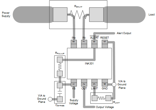
INA301 ai_layout_bos713.gif

NOTE:

Connect the limit resistor directly to the GND pin.
Figure 44. Recommended Layout