ZHCSEK8A September 2015 – February 2016 INA301
PRODUCTION DATA.
- 1 特性
- 2 应用范围
- 3 说明
- 4 修订历史记录
- 5 Pin Configuration and Functions
- 6 Specifications
- 7 Detailed Description
- 8 Applications and Implementation
- 9 Power Supply Recommendations
- 10Layout
- 11器件和文档支持
- 12机械、封装和可订购信息
6 Specifications
6.1 Absolute Maximum Ratings
over operating free-air temperature range (unless otherwise noted)(1)| MIN | MAX | UNIT | ||
|---|---|---|---|---|
| Supply voltage, VS | 6 | V | ||
| Analog inputs (IN+, IN–) | Differential (VIN+) – (VIN–)(2) | –40 | 40 | V |
| Common-mode(3) | GND – 0.3 | 40 | ||
| Analog input | LIMIT pin | GND – 0.3 | (VS) + 0.3 | V |
| Analog output | OUT pin | GND – 0.3 | (VS) + 0.3 | V |
| Digital input | RESET pin | GND – 0.3 | (VS) + 0.3 | V |
| Digital output | ALERT pin | GND – 0.3 | 6 | V |
| Junction temperature, TJ | 150 | °C | ||
| Storage temperature, Tstg | –65 | 150 | °C | |
(1) Stresses beyond those listed under Absolute Maximum Ratings may cause permanent damage to the device. These are stress ratings only, which do not imply functional operation of the device at these or any other conditions beyond those indicated under Recommended Operating Conditions. Exposure to absolute-maximum-rated conditions for extended periods may affect device reliability.
(2) VIN+ and VIN– are the voltages at the IN+ and IN– pins, respectively.
(3) Input voltage can exceed the voltage shown without causing damage to the device if the current at that pin is limited to 5 mA.
6.2 ESD Ratings
| VALUE | UNIT | |||
|---|---|---|---|---|
| V(ESD) | Electrostatic discharge | Human-body model (HBM), per ANSI/ESDA/JEDEC JS-001(1) | ±2000 | V |
| Charged-device model (CDM), per JEDEC specification JESD22-C101(2) | ±1000 | |||
(1) JEDEC document JEP155 states that 500-V HBM allows safe manufacturing with a standard ESD control process.
(2) JEDEC document JEP157 states that 250-V CDM allows safe manufacturing with a standard ESD control process.
6.3 Recommended Operating Conditions
over operating free-air temperature range (unless otherwise noted)| MIN | NOM | MAX | UNIT | ||
|---|---|---|---|---|---|
| VCM | Common-mode input voltage | 12 | V | ||
| VS | Operating supply voltage | 5 | V | ||
| TA | Operating free-air temperature | –40 | 125 | °C | |
6.4 Thermal Information
| THERMAL METRIC(1) | INA301 | UNIT | |
|---|---|---|---|
| DGK (MSOP) | |||
| 8 PINS | |||
| RθJA | Junction-to-ambient thermal resistance | 161.5 | °C/W |
| RθJC(top) | Junction-to-case (top) thermal resistance | 62.3 | °C/W |
| RθJB | Junction-to-board thermal resistance | 81.4 | °C/W |
| ψJT | Junction-to-top characterization parameter | 6.8 | °C/W |
| ψJB | Junction-to-board characterization parameter | 80 | °C/W |
| RθJC(bot) | Junction-to-case (bottom) thermal resistance | N/A | °C/W |
(1) For more information about traditional and new thermal metrics, see the Semiconductor and IC Package Thermal Metrics application report, SPRA953.
6.5 Electrical Characteristics
at TA = 25°C, VSENSE = VIN+ – VIN– = 10 mV, VS = 5 V, VIN+ = 12 V, and VLIMIT = 2 V (unless otherwise noted)| PARAMETER | TEST CONDITIONS | MIN | TYP | MAX | UNIT | |
|---|---|---|---|---|---|---|
| INPUT | ||||||
| VCM | Common-mode input voltage range | 0 | 36 | V | ||
| VIN | Differential input voltage range | VIN = VIN+ – VIN–, INA301A1 | 0 | 250 | mV | |
| VIN = VIN+ – VIN–, INA301A2 | 0 | 100 | ||||
| VIN = VIN+ – VIN–, INA301A3 | 0 | 50 | ||||
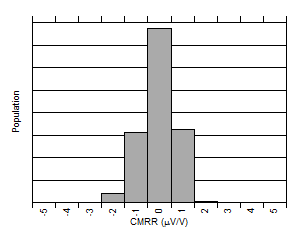
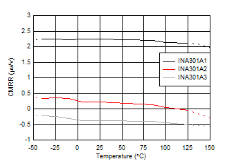
| CMR | Common-mode rejection | INA301A1, VIN+ = 0 V to 36 V, TA = –40ºC to +125ºC |
100 | 110 | dB | |
| INA301A2, VIN+ = 0 V to 36 V, TA = –40ºC to +125ºC |
106 | 118 | ||||
| INA301A3, VIN+ = 0 V to 36 V, TA = –40ºC to +125ºC |
110 | 120 | ||||
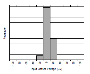
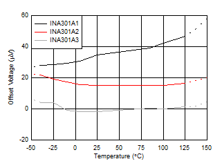
| VOS | Offset voltage, RTI(1) | INA301A1 | ±25 | ±125 | µV | |
| INA301A2 | ±15 | ±50 | ||||
| INA301A3 | ±10 | ±35 | ||||
| dVOS/dT | Offset voltage drift, RTI(1) | TA= –40ºC to +125ºC | 0.1 | 0.5 | µV/°C | |
| PSRR | Power-supply rejection ratio | VS = 2.7 V to 5.5 V, VIN+ = 12 V, TA = –40ºC to +125ºC |
±0.1 | ±10 | µV/V | |
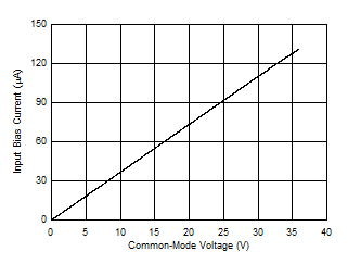
| IB | Input bias current | IB+, IB– | 120 | µA | ||
| IOS | Input offset current | VSENSE = 0 mV | ±0.1 | µA | ||
| OUTPUT | ||||||
| G | Gain | INA301A1 | 20 | V/V | ||
| INA301A2 | 50 | |||||
| INA301A3 | 100 | |||||
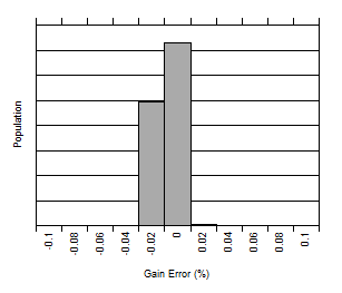
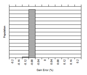
| Gain error | INA301A1, VOUT = 0.5 V to VS – 0.5 V | ±0.03% | ±0.1% | |||
| INA301A2, VOUT = 0.5 V to VS – 0.5 V | ±0.05% | ±0.15% | ||||
| INA301A3, VOUT = 0.5 V to VS – 0.5 V | ±0.11% | ±0.2% | ||||
| TA= –40ºC to 125ºC | 3 | 10 | ppm/°C | |||
| Nonlinearity error | VOUT = 0.5 V to VS – 0.5 V | ±0.01% | ||||
| Maximum capacitive load | No sustained oscillation | 500 | pF | |||
| VOLTAGE OUTPUT | ||||||
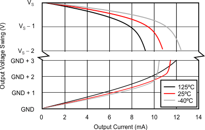
| Swing to VS power-supply rail | RL = 10 kΩ to GND, TA = –40ºC to +125ºC |
VS – 0.05 | VS – 0.1 | V | ||
| Swing to GND | RL = 10 kΩ to GND, TA = –40ºC to +125ºC |
VGND + 20 | VGND + 30 | mV | ||
| FREQUENCY RESPONSE | ||||||
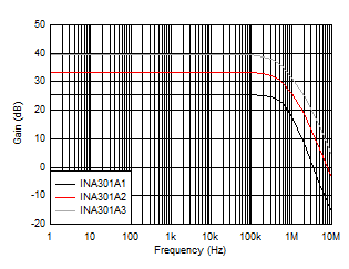
| BW | Bandwidth | INA301A1 | 550 | kHz | ||
| INA301A2 | 500 | |||||
| INA301A3 | 450 | |||||
| SR | Slew rate | 4 | V/µs | |||
| NOISE, RTI(1) | ||||||
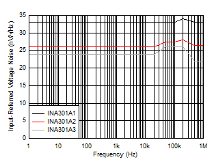
| Voltage noise density | 30 | nV/√Hz | ||||
| COMPARATOR | ||||||
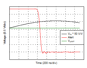
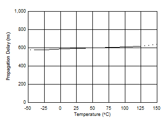
| tp | Total alert propagation delay | Input overdrive = 1 mV | 0.75 | 1 | µs | |
| Slew-rate-limited tp | VOUT step = 0.5 V to 4.5 V, VLIMIT = 4 V | 1 | 1.5 | |||
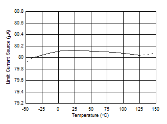
| ILIMIT | Limit threshold output current | TA = 25ºC | 79.7 | 80 | 80.3 | µA |
| TA = –40ºC to +125ºC | 79.2 | 80.8 | ||||
| VOS | Comparator offset voltage | INA301A1 | 1 | 3.5 | mV | |
| INA301A2 | 1 | 4 | ||||
| INA301A3 | 1.5 | 4.5 | ||||
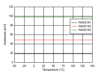
| HYS | Hysteresis | INA301A1 | 20 | mV | ||
| INA301A2 | 50 | |||||
| INA301A3 | 100 | |||||
| VIH | High-level input voltage | 1.4 | 6 | V | ||
| VIL | Low-level input voltage | 0 | 0.4 | V | ||
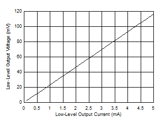
| VOL | Alert low-level output voltage | IOL = 3 mA | 70 | 300 | mV | |
| ALERT pin leakage input current | VOH = 3.3 V | 0.1 | 1 | µA | ||
| Digital leakage input current | 0 ≤ VIN ≤ VS | 1 | µA | |||
| POWER SUPPLY | ||||||
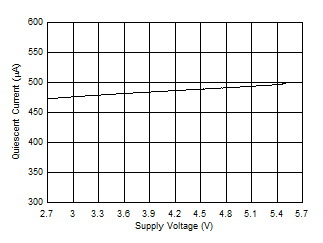
| VS | Operating supply range | TA = –40ºC to +125ºC | 2.7 | 5.5 | V | |
| IQ | Quiescent current | VSENSE = 0 mV, TA = 25ºC | 500 | 650 | µA | |
| TA = –40ºC to +125ºC | 700 | |||||
| TEMPERATURE RANGE | ||||||
| Specified range | –40 | 125 | °C | |||
(1) RTI = referred-to-input.
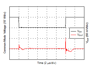
6.6 Typical Characteristics
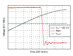
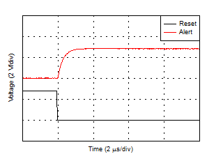
at TA = 25°C, VS = 5 V, VIN+ = 12 V, and alert pullup resistor = 10 kΩ (unless otherwise noted)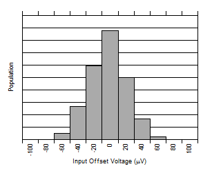
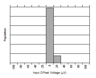
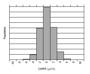
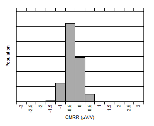
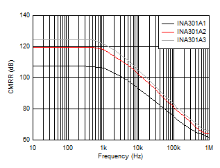
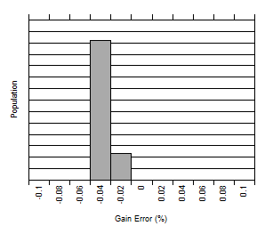
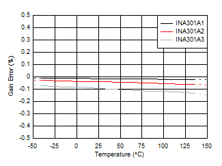
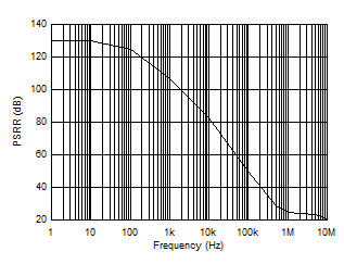
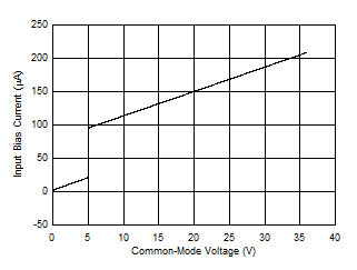
(VS = 5 V)
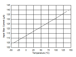
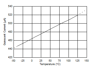
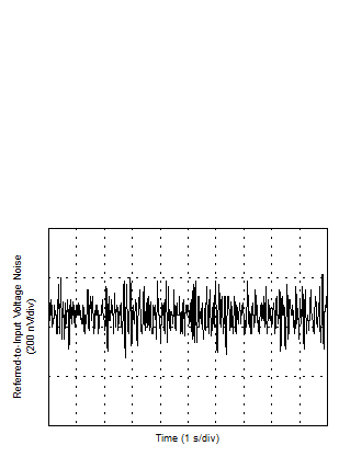
(Referred-to-Input)
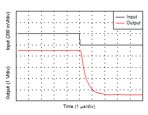
(4-VPP Output Step)
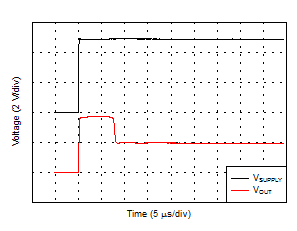
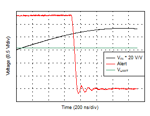
(VS = 0 V)
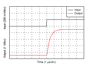
(4-VPP Output Step)
