ZHCSH47 November   2017 INA317

PRODUCTION DATA.  

  1. 特性
  2. 应用
  3. 说明
    1.     Device Images
      1.      简化原理图
  4. 修订历史记录
  5. Pin Configuration and Functions
    1.     Pin Functions
  6. Specifications
    1. 6.1 Absolute Maximum Ratings
    2. 6.2 ESD Ratings
    3. 6.3 Recommended Operating Conditions
    4. 6.4 Thermal Information
    5. 6.5 Electrical Characteristics
    6. 6.6 Typical Characteristics
  7. Detailed Description
    1. 7.1 Overview
    2. 7.2 Functional Block Diagram
    3. 7.3 Feature Description
    4. 7.4 Device Functional Modes
      1. 7.4.1 Internal Offset Correction
      2. 7.4.2 Input Common-Mode Range
  8. Application and Implementation
    1. 8.1 Application Information
    2. 8.2 Typical Application
      1. 8.2.1 Design Requirements
      2. 8.2.2 Detailed Design Procedure
        1. 8.2.2.1  Setting the Gain
        2. 8.2.2.2  Internal Offset Correction
        3. 8.2.2.3  Offset Trimming
        4. 8.2.2.4  Noise Performance
        5. 8.2.2.5  Input Bias Current Return Path
        6. 8.2.2.6  Input Common-Mode Range
        7. 8.2.2.7  Operating Voltage
        8. 8.2.2.8  Low Voltage Operation
        9. 8.2.2.9  Single-Supply Operation
        10. 8.2.2.10 Input Protection
      3. 8.2.3 Application Curves
  9. Power Supply Recommendations
  10. 10Layout
    1. 10.1 Layout Guidelines
    2. 10.2 Layout Example
  11. 11器件和文档支持
    1. 11.1 器件支持
      1. 11.1.1 开发支持
        1. 11.1.1.1 TINA-TI(免费下载软件)
    2. 11.2 文档支持
      1. 11.2.1 相关文档
    3. 11.3 商标
    4. 11.4 静电放电警告
    5. 11.5 Glossary
  12. 12机械、封装和可订购信息

封装选项

机械数据 (封装 | 引脚)
散热焊盘机械数据 (封装 | 引脚)
订购信息

Typical Application

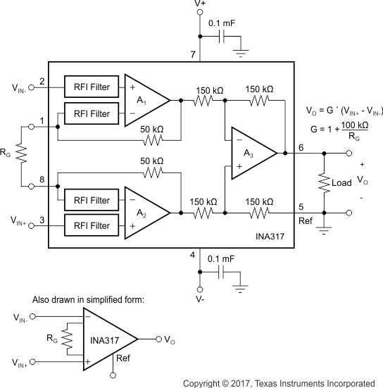
Figure 32 shows the basic connections required for operation of the INA317 device. Good layout practice mandates the use of bypass capacitors placed close to the device pins as shown.

The output of the INA317 device is referred to the output reference (REF) pin, which is normally grounded. This connection must be low-impedance to ensure good common-mode rejection. Although 15 Ω or less of stray resistance is tolerated while maintaining specified CMRR, small stray resistances of tens of ohms in series with the REF pin causes noticeable degradation in CMRR.
INA317 ai_basic_connex_bos445.gifFigure 32. Basic Connections