ZHCSH47 November 2017 INA317
PRODUCTION DATA.
- 1 特性
- 2 应用
- 3 说明
- 4 修订历史记录
- 5 Pin Configuration and Functions
- 6 Specifications
- 7 Detailed Description
- 8 Application and Implementation
- 9 Power Supply Recommendations
- 10Layout
- 11器件和文档支持
- 12机械、封装和可订购信息
8.2.2.5 Input Bias Current Return Path
The input impedance of the INA317 device is extremely high(approximately 100 GΩ.) However, a path must be provided for the input bias current of the inputs. This input bias current is typically ±70 pA. High-input impedance means that this input bias current changes very little with varying input voltage.
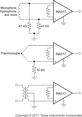
For proper operation, input circuitry must provide a path for the input bias current. Figure 34 shows various provisions for an input bias current path. Without a bias current path, the inputs float to a potential that exceeds the common-mode range of the INA317 device, and the input amplifiers saturate. If the differential source resistance is low, the bias current return path connects to one input (see the thermocouple example in Figure 34). With higher source impedance, using two equal resistors provides a balanced input with possible advantages of lower input offset voltage as a result of bias current and better high-frequency common-mode rejection.
 Figure 34. Providing an Input Common-Mode Current Path