ZHCSKC7B september 2019 – june 2023 INA333-Q1
PRODUCTION DATA
- 1
- 1 特性
- 2 应用
- 3 说明
- 4 Revision History
- 5 Pin Configuration and Functions
- 6 Specifications
- 7 Detailed Description
- 8 Application and Implementation
- 9 Device and Documentation Support
- 10Mechanical, Packaging, and Orderable Information
8.2.2.4 Input Bias Current Return Path
The input impedance of the INA333-Q1 is extremely high; approximately 100 GΩ. However, a path must be provided for the input bias current of both inputs. This input bias current is typically ±70 pA. High input impedance means that this input bias current changes very little with varying input voltage.
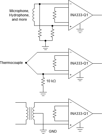
Input circuitry must provide a path for this input bias current for proper operation. Figure 8-3 shows various provisions for an input bias current path. Without a bias current path, the inputs float to a potential that exceeds the common-mode range of the device, and the input amplifiers saturate. If the differential source resistance is low, the bias current return path can be connected to one input (see the thermocouple example in Figure 8-3). With higher source impedance, use two equal resistors to provide a balanced input with the possible advantages of a lower input offset voltage as a result of bias current, and improved high-frequency common-mode rejection.
 Figure 8-3 Providing an Input Common-Mode Current Path