ZHCSKC7B september   2019  – june 2023 INA333-Q1

PRODUCTION DATA  

  1.   1
  2. 特性
  3. 应用
  4. 说明
  5. Revision History
  6. Pin Configuration and Functions
  7. Specifications
    1. 6.1 Absolute Maximum Ratings
    2. 6.2 ESD Ratings
    3. 6.3 Recommended Operating Conditions
    4. 6.4 Thermal Information
    5. 6.5 Electrical Characteristics
    6. 6.6 Typical Characteristics
  8. Detailed Description
    1. 7.1 Overview
    2. 7.2 Functional Block Diagram
    3. 7.3 Feature Description
      1. 7.3.1 Internal Offset Correction
      2. 7.3.2 Input Protection
    4. 7.4 Device Functional Modes
  9. Application and Implementation
    1. 8.1 Application Information
      1. 8.1.1 Input Common-Mode Range
    2. 8.2 Typical Application
      1. 8.2.1 Design Requirements
      2. 8.2.2 Detailed Design Procedure
        1. 8.2.2.1 Setting the Gain
        2. 8.2.2.2 Offset Trimming
        3. 8.2.2.3 Noise Performance
        4. 8.2.2.4 Input Bias Current Return Path
        5. 8.2.2.5 Low Voltage Operation
        6. 8.2.2.6 Single-Supply Operation
      3. 8.2.3 Application Curves
    3. 8.3 Power Supply Recommendations
    4. 8.4 Layout
      1. 8.4.1 Layout Guidelines
      2. 8.4.2 Layout Example
  10. Device and Documentation Support
    1. 9.1 Device Support
      1. 9.1.1 Development Support
        1. 9.1.1.1 TINA-TI Simulation Software (Free Download)
    2. 9.2 Documentation Support
      1. 9.2.1 Related Documentation
    3. 9.3 接收文档更新通知
    4. 9.4 支持资源
    5. 9.5 Trademarks
    6. 9.6 静电放电警告
    7. 9.7 术语表
  11. 10Mechanical, Packaging, and Orderable Information

封装选项

机械数据 (封装 | 引脚)
散热焊盘机械数据 (封装 | 引脚)
订购信息

Typical Application

Figure 8-1 shows the basic connections required for operation of the INA333-Q1. Good layout practice mandates the use of bypass capacitors placed close to the device pins as shown.

The output of the INA333-Q1 is referred to the output reference (REF) pin, which is normally grounded. This connection must be low-impedance to maintain good common-mode rejection. Although 15 Ω or less of stray resistance can be tolerated while maintaining specified CMRR, small stray resistances of tens of ohms in series with the REF pin can cause noticeable degradation in CMRR.
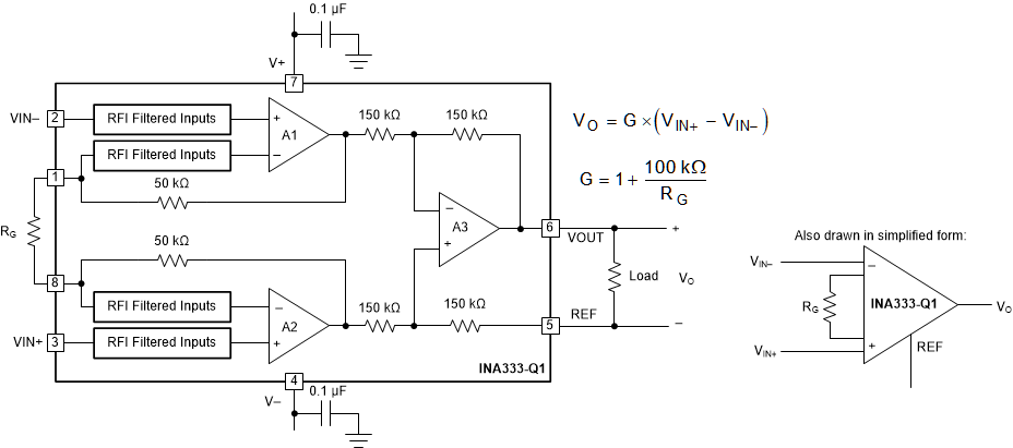
GUID-BD9B0A07-1CCC-4E69-B333-F3760A31C46C-low.gifFigure 8-1 Basic Connections