ZHCSKC7B september   2019  – june 2023 INA333-Q1

PRODUCTION DATA  

  1.   1
  2. 特性
  3. 应用
  4. 说明
  5. Revision History
  6. Pin Configuration and Functions
  7. Specifications
    1. 6.1 Absolute Maximum Ratings
    2. 6.2 ESD Ratings
    3. 6.3 Recommended Operating Conditions
    4. 6.4 Thermal Information
    5. 6.5 Electrical Characteristics
    6. 6.6 Typical Characteristics
  8. Detailed Description
    1. 7.1 Overview
    2. 7.2 Functional Block Diagram
    3. 7.3 Feature Description
      1. 7.3.1 Internal Offset Correction
      2. 7.3.2 Input Protection
    4. 7.4 Device Functional Modes
  9. Application and Implementation
    1. 8.1 Application Information
      1. 8.1.1 Input Common-Mode Range
    2. 8.2 Typical Application
      1. 8.2.1 Design Requirements
      2. 8.2.2 Detailed Design Procedure
        1. 8.2.2.1 Setting the Gain
        2. 8.2.2.2 Offset Trimming
        3. 8.2.2.3 Noise Performance
        4. 8.2.2.4 Input Bias Current Return Path
        5. 8.2.2.5 Low Voltage Operation
        6. 8.2.2.6 Single-Supply Operation
      3. 8.2.3 Application Curves
    3. 8.3 Power Supply Recommendations
    4. 8.4 Layout
      1. 8.4.1 Layout Guidelines
      2. 8.4.2 Layout Example
  10. Device and Documentation Support
    1. 9.1 Device Support
      1. 9.1.1 Development Support
        1. 9.1.1.1 TINA-TI Simulation Software (Free Download)
    2. 9.2 Documentation Support
      1. 9.2.1 Related Documentation
    3. 9.3 接收文档更新通知
    4. 9.4 支持资源
    5. 9.5 Trademarks
    6. 9.6 静电放电警告
    7. 9.7 术语表
  11. 10Mechanical, Packaging, and Orderable Information

封装选项

机械数据 (封装 | 引脚)
散热焊盘机械数据 (封装 | 引脚)
订购信息

Single-Supply Operation

The INA333-Q1 can be used on single power supplies of 1.8 V to 5.5 V. Figure 8-4 shows a basic single-supply circuit. The output REF pin is connected to midsupply. Zero differential input voltage demands an output voltage of midsupply. Actual output voltage swing is limited to approximately 50 mV more than ground, when the load is referred to ground as shown. Figure 6-29 shows how the output voltage swing varies with output current.

With single-supply operation, VIN+ and VIN– must both be 0.1 V greater than ground for linear operation. For instance, the inverting input cannot be connected to ground to measure a voltage connected to the noninverting input.

To show the issues affecting low-voltage operation, consider the circuit in Figure 8-4 that shows the device operating from a single 3-V supply. A resistor in series with the low side of the bridge makes sure that the bridge output voltage is within the common-mode range of the amplifier inputs.
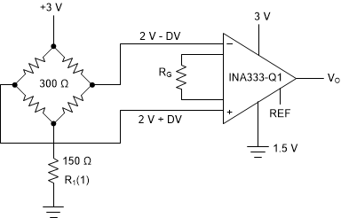
GUID-3D442701-DAFA-4E04-9A33-CA2A15AB25F9-low.gif
(1) R1 creates proper common-mode voltage, only for low-voltage operation; see Section 8.2.2.6.
Figure 8-4 Single-Supply Bridge Amplifier