ZHCSAK0C July 2008 – December 2015 INA333
PRODUCTION DATA.
- 1 特性
- 2 应用范围
- 3 说明
- 4 修订历史记录
- 5 Pin Configuration and Functions
- 6 Specifications
- 7 Detailed Description
- 8 Application and Implementation
- 9 Power Supply Recommendations
- 10Layout
- 11器件和文档支持
- 12机械、封装和可订购信息
封装选项
机械数据 (封装 | 引脚)
散热焊盘机械数据 (封装 | 引脚)
- DRG|8
订购信息
6 Specifications
6.1 Absolute Maximum Ratings
over operating free-air temperature range (unless otherwise noted) (1)| MIN | MAX | UNIT | ||
|---|---|---|---|---|
| Supply voltage | 7 | V | ||
| Analog input voltage(2) | (V–) – 0.3 | (V+) + 0.3 | V | |
| Output short-circuit(3) | Continuous | |||
| Operating temperature, TA | –40 | 150 | °C | |
| Junction temperature, TJ | 150 | °C | ||
| Storage temperature, Tstg | –65 | 150 | °C | |
(1) Stresses beyond those listed under Absolute Maximum Ratings may cause permanent damage to the device. These are stress ratings only, which do not imply functional operation of the device at these or any other conditions beyond those indicated under Recommended Operating Conditions. Exposure to absolute-maximum-rated conditions for extended periods may affect device reliability.
(2) Input pins are diode-clamped to the power-supply rails. Input signals that can swing more than 0.3 V beyond the supply rails should be current limited to 10 mA or less.
(3) Short-circuit to ground.
6.2 ESD Ratings
| VALUE | UNIT | |||
|---|---|---|---|---|
| V(ESD) | Electrostatic discharge | Human-body model (HBM), per ANSI/ESDA/JEDEC JS-001(1) | ±4000 | V |
| Charged-device model (CDM), per JEDEC specification JESD22-C101(2) | ±1000 | |||
| Machine model (MM) | ±200 | |||
(1) JEDEC document JEP155 states that 500-V HBM allows safe manufacturing with a standard ESD control process.
(2) JEDEC document JEP157 states that 250-V CDM allows safe manufacturing with a standard ESD control process.
6.3 Recommended Operating Conditions
over operating free-air temperature range (unless otherwise noted)| MIN | MAX | UNIT | ||
|---|---|---|---|---|
| VS | Supply voltage | 1.8 | 5.5 | V |
| Specified temperature | –40 | 125 | °C | |
6.4 Thermal Information
| THERMAL METRIC(1) | INA333 | UNIT | ||
|---|---|---|---|---|
| DGK (VSSOP) | DRG (WSON) | |||
| 8 PINS | 8 PINS | |||
| RθJA | Junction-to-ambient thermal resistance | 169.5 | 60 | °C/W |
| RθJC(top) | Junction-to-case (top) thermal resistance | 62.7 | 60 | °C/W |
| RθJB | Junction-to-board thermal resistance | 90.3 | 50 | °C/W |
| ψJT | Junction-to-top characterization parameter | 7.6 | — | °C/W |
| ψJB | Junction-to-board characterization parameter | 88.7 | — | °C/W |
| RθJC(bot) | Junction-to-case (bottom) thermal resistance | — | 6 | °C/W |
(1) For more information about traditional and new thermal metrics, see the Semiconductor and IC Package Thermal Metrics application report, SPRA953.
6.5 Electrical Characteristics
for VS = 1.8 V to 5.5 V at TA = 25°C, RL = 10 kΩ, VREF = VS / 2, and G = 1 (unless otherwise noted)| PARAMETER | TEST CONDITIONS | MIN | TYP | MAX | UNIT | ||
|---|---|---|---|---|---|---|---|
| INPUT(1) | |||||||
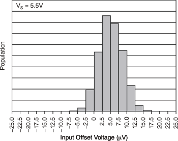
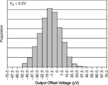
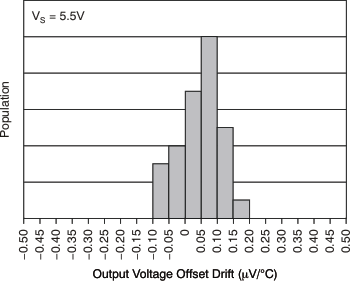
| VOSI | Offset voltage, RTI(2) | ±10 ±25/G | ±25 ±75/G | μV | |||
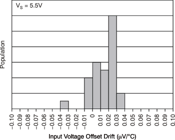
| PSR | vs temperature | TA = –40°C to +125°C | ±0.1 ±0.5 / G | μV/°C | |||
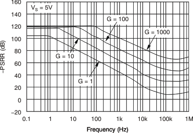
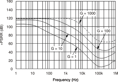
| vs power supply | 1.8 V ≤ VS ≤ 5.5 V | ±1 ±5/G | ±5 ±15/G | μV/V | |||
| Long-term stability | See (3) | ||||||
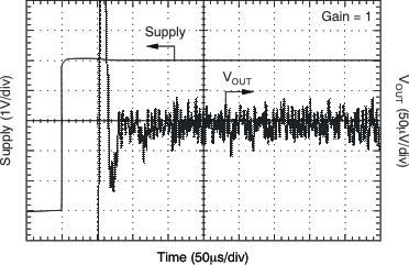
| Turnon time to specified VOSI | TA = –40°C to +125°C | See Typical Characteristics | |||||
| Impedance | |||||||
| ZIN | Differential | 100 || 3 | GΩ || pF | ||||
| ZIN | Common-mode | 100 || 3 | GΩ || pF | ||||
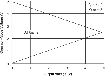
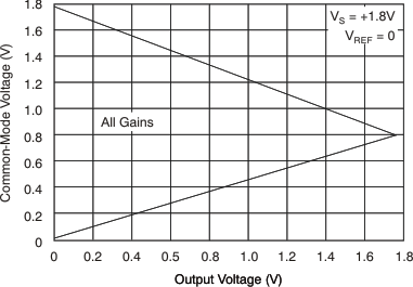
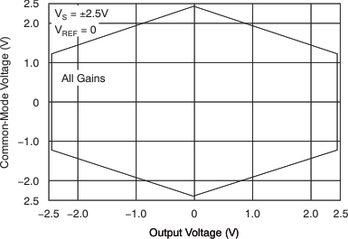
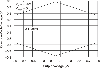
| VCM | Common-mode voltage range | VO = 0 V | (V–) + 0.1 | (V+) – 0.1 | V | ||
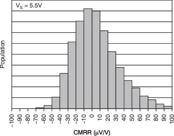
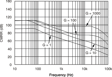
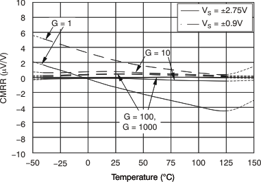
| CMR | Common-mode rejection | DC to 60 Hz | |||||
| G = 1 | VCM = (V–) + 0.1 V to (V+) – 0.1 V |
80 | 90 | dB | |||
| G = 10 | VCM = (V–) + 0.1 V to (V+) – 0.1 V |
100 | 110 | dB | |||
| G = 100 | VCM = (V–) + 0.1 V to (V+) – 0.1 V |
100 | 115 | dB | |||
| G = 1000 | VCM = (V–) + 0.1 V to (V+) – 0.1 V |
100 | 115 | dB | |||
| INPUT BIAS CURRENT | |||||||
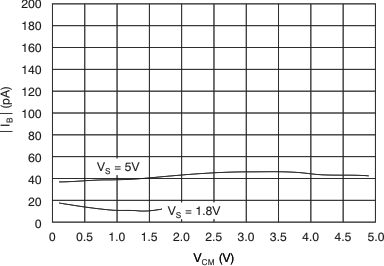
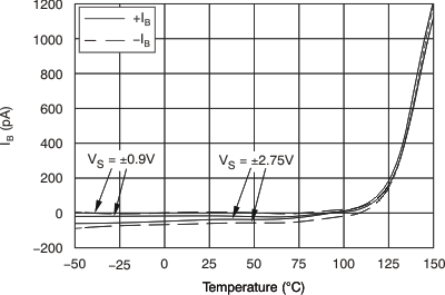
| IB | Input bias current | ±70 | ±200 | pA | |||
| vs temperature | TA = –40°C to +125°C | See Figure 26 | pA/°C | ||||
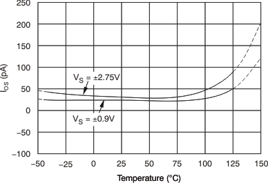
| IOS | Input offset current | ±50 | ±200 | pA | |||
| vs temperature | TA = –40°C to +125°C | See Figure 28 | pA/°C | ||||
| INPUT VOLTAGE NOISE | |||||||
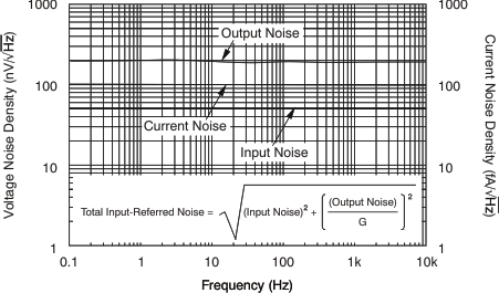
| eNI | Input voltage noise | G = 100, RS = 0 Ω, f = 10 Hz | 50 | nV/√Hz | |||
| G = 100, RS = 0 Ω, f = 100 Hz | 50 | nV/√Hz | |||||
| G = 100, RS = 0 Ω, f = 1 kHz | 50 | nV/√Hz | |||||
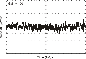
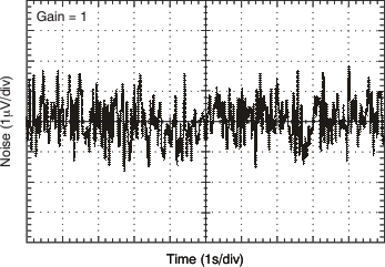
| G = 100, RS = 0 Ω, f = 0.1 Hz to 10 Hz | 1 | μVPP | |||||
| iN | Input current noise | f = 10 Hz | 100 | fA/√Hz | |||
| f = 0.1 Hz to 10 Hz | 2 | pAPP | |||||
| GAIN | |||||||
| G | Gain equation | 1 + (100 kΩ/RG) | V/V | ||||
| Range of gain | 1 | 1000 | V/V | ||||
| Gain error | VS = 5.5 V, (V–) + 100 mV ≤ VO ≤ (V+) – 100 mV |
||||||
| G = 1 | ±0.01% | ±0.1% | |||||
| G = 10 | ±0.05% | ±0.25% | |||||
| G = 100 | ±0.07% | ±0.25% | |||||
| G = 1000 | ±0.25% | ±0.5% | |||||
| Gain vs temperature, G = 1 | TA = –40°C to +125°C | ±1 | ±5 | ppm/°C | |||
| Gain vs temperature, G > 1(4) | TA = –40°C to +125°C | ±15 | ±50 | ppm/°C | |||
| Gain nonlinearity | VS = 5.5 V, (V–) + 100 mV ≤ VO ≤ (V+) – 100 mV |
||||||
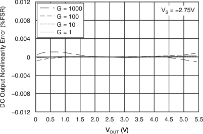
| Gain nonlinearity, G = 1 to 1000 | RL = 10 kΩ | 10 | ppm | ||||
| OUTPUT | |||||||
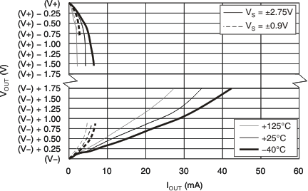
| Output voltage swing from rail | VS = 5.5 V, RL = 10 kΩ | See Figure 29 | 50 | mV | |||
| Capacitive load drive | 500 | pF | |||||
| ISC | Short-circuit current | Continuous to common | –40, +5 | mA | |||
| FREQUENCY RESPONSE | |||||||
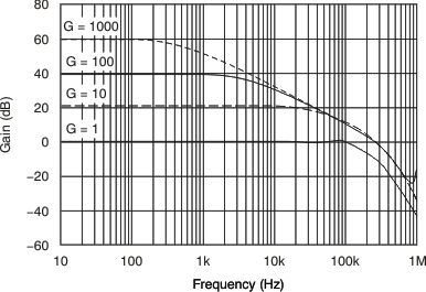
| Bandwidth, –3dB | G = 1 | 150 | kHz | ||||
| G = 10 | 35 | kHz | |||||
| G = 100 | 3.5 | kHz | |||||
| G = 1000 | 350 | Hz | |||||
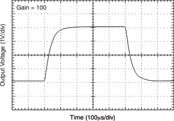
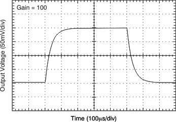
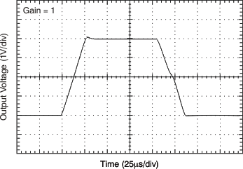
| SR | Slew rate | VS = 5 V, VO = 4-V step, G = 1 | 0.16 | V/μs | |||
| VS = 5 V, VO = 4-V step, G = 100 | 0.05 | V/μs | |||||
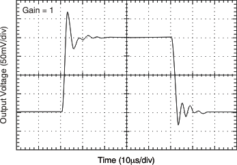
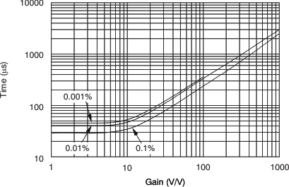
| tS | Settling time to 0.01% | VSTEP = 4 V, G = 1 | 50 | μs | |||
| VSTEP = 4 V, G = 100 | 400 | μs | |||||
| tS | Settling time to 0.001% | VSTEP = 4 V, G = 1 | 60 | μs | |||
| VSTEP = 4 V, G = 100 | 500 | μs | |||||
| Overload recovery | 50% overdrive | 75 | μs | ||||
| REFERENCE INPUT | |||||||
| RIN | 300 | kΩ | |||||
| Voltage range | V– | V+ | V | ||||
| POWER SUPPLY | |||||||
| Voltage range | Single voltage range | +1.8 | +5.5 | V | |||
| Dual voltage range | ±0.9 | ±2.75 | V | ||||
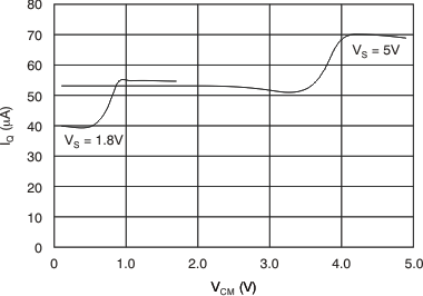
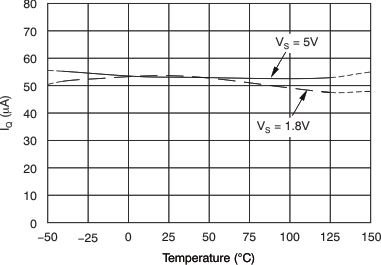
| IQ | Quiescent current | VIN = VS / 2 | 50 | 75 | μA | ||
| vs temperature | TA = –40°C to +125°C | 80 | μA | ||||
| TEMPERATURE RANGE | |||||||
| Specified temperature range | –40 | 125 | °C | ||||
| Operating temperature range | –40 | 150 | °C | ||||
(1) Total VOS, referred-to-input = (VOSI) + (VOSO / G)
(2) RTI = Referred-to-input
(3) 300-hour life test at 150°C demonstrated randomly distributed variation of approximately 1 μV
(4) Does not include effects of external resistor RG
6.6 Typical Characteristics
at TA = 25°C, VS = 5 V, RL = 10 kΩ, VREF = midsupply, and G = 1 (unless otherwise noted)