ZHCSIM8C August   2018  – July 2019 INA821

PRODUCTION DATA.  

  1. 特性
  2. 应用
  3. 说明
    1.     Device Images
      1.      INA821 简化内部原理图
      2.      输入阶段失调电压漂移的典型分布
  4. 修订历史记录
  5. Device Comparison Table
  6. Pin Configuration and Functions
    1.     Pin Functions
  7. Specifications
    1. 7.1 Absolute Maximum Ratings
    2. 7.2 ESD Ratings
    3. 7.3 Recommended Operating Conditions
    4. 7.4 Thermal Information
    5. 7.5 Electrical Characteristics
    6. 7.6 Typical Characteristics: Table of Graphs
    7. 7.7 Typical Characteristics
  8. Detailed Description
    1. 8.1 Overview
    2. 8.2 Functional Block Diagram
    3. 8.3 Feature Description
      1. 8.3.1 Setting the Gain
        1. 8.3.1.1 Gain Drift
      2. 8.3.2 EMI Rejection
      3. 8.3.3 Input Common-Mode Range
      4. 8.3.4 Input Protection
      5. 8.3.5 Operating Voltage
      6. 8.3.6 Error Sources
    4. 8.4 Device Functional Modes
  9. Application and Implementation
    1. 9.1 Application Information
      1. 9.1.1 Reference Pin
      2. 9.1.2 Input Bias Current Return Path
    2. 9.2 Typical Application
      1. 9.2.1 Design Requirements
      2. 9.2.2 Detailed Design Procedure
      3. 9.2.3 Application Curves
    3. 9.3 Other Application Examples
      1. 9.3.1 Resistance Temperature Detector Interface
  10. 10Power Supply Recommendations
  11. 11Layout
    1. 11.1 Layout Guidelines
    2. 11.2 Layout Example
  12. 12器件和文档支持
    1. 12.1 器件支持
      1. 12.1.1 开发支持
    2. 12.2 文档支持
      1. 12.2.1 相关文档
    3. 12.3 接收文档更新通知
    4. 12.4 社区资源
    5. 12.5 商标
    6. 12.6 静电放电警告
    7. 12.7 Glossary
  13. 13机械、封装和可订购信息

封装选项

机械数据 (封装 | 引脚)
散热焊盘机械数据 (封装 | 引脚)
订购信息

Typical Characteristics

at TA = 25°C, VS = ±15 V, RL = 10 kΩ, VREF = 0 V, and G = 1 (unless otherwise noted)
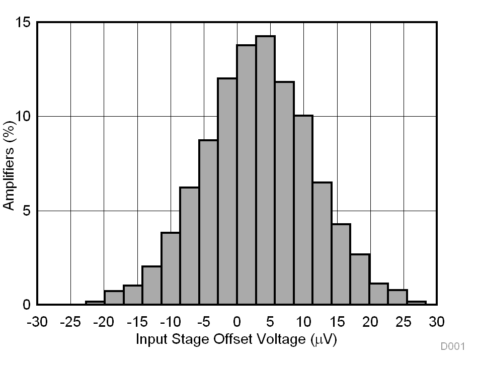
INA821 D001_INA821.gif
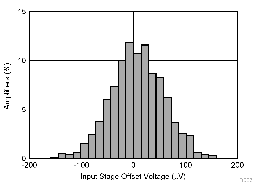
N = 2667 Mean = 3.1 µV Std. Dev. = 8.1 µV
Figure 1. Typical Distribution of
Input Stage Offset Voltage
INA821 D003_INA821.gif
N = 2667 Mean = 7.7 µV Std. Dev. = 50.7 µV
Figure 3. Typical Distribution of
Output Stage Offset Voltage
INA821 D005_INA821.gif
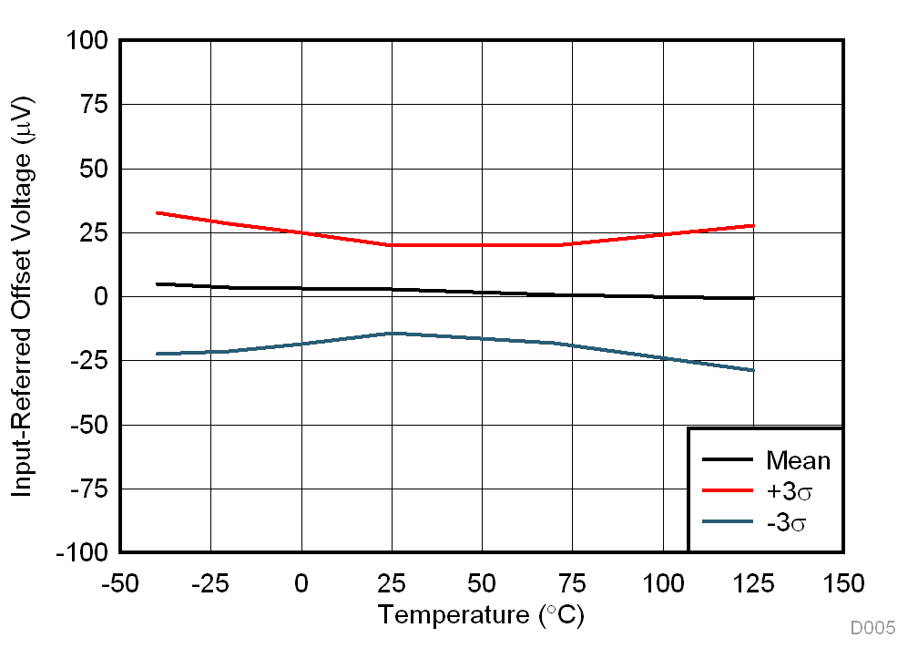
81 units
Figure 5. Input Stage Offset Voltage vs Temperature
INA821 D007_INA821.gif
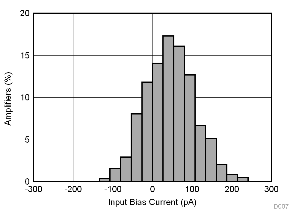
N = 292 Mean = 45 pA Std. Dev. = 62 pA
TA = 25°C
Figure 7. Typical Distribution of Input Bias Current,
TA = 25°C
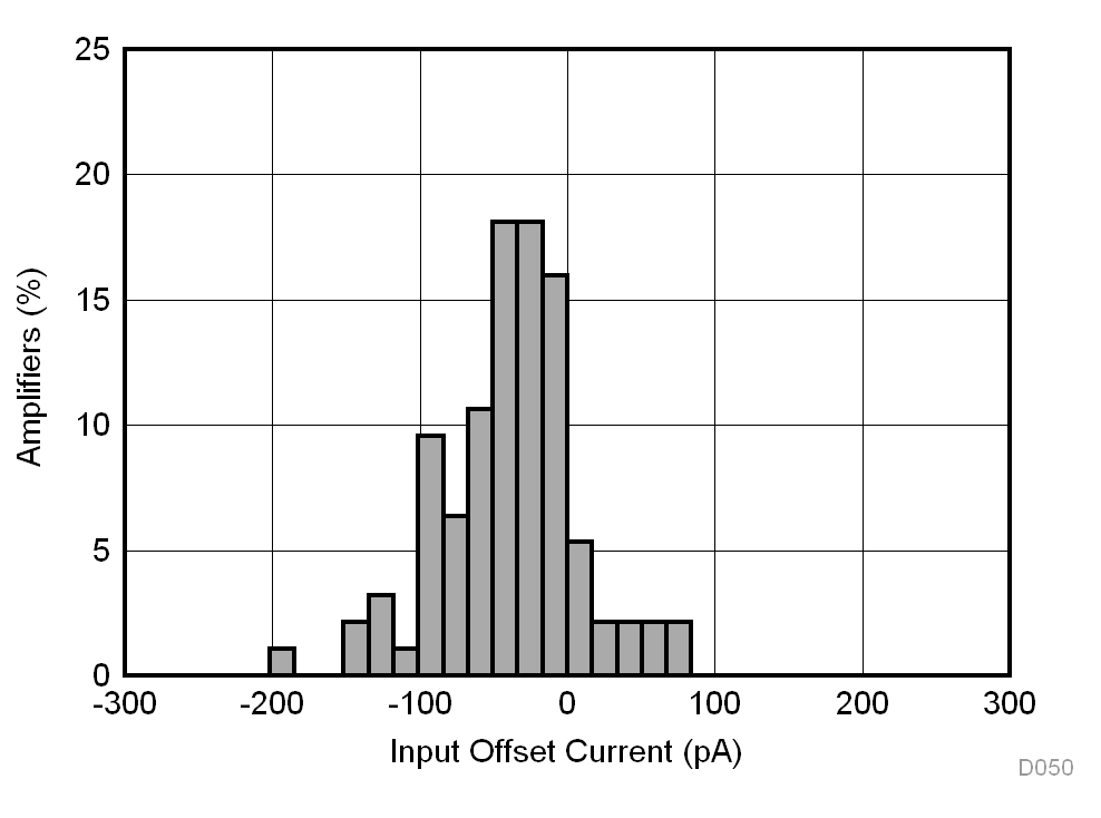
INA821 D050_INA821.gif
N = 94 Mean = –38.82 pA Std. Dev. = 47.24 pA
Figure 9. Typical Distribution of Input Offset Current
INA821 D010_INA821.gif
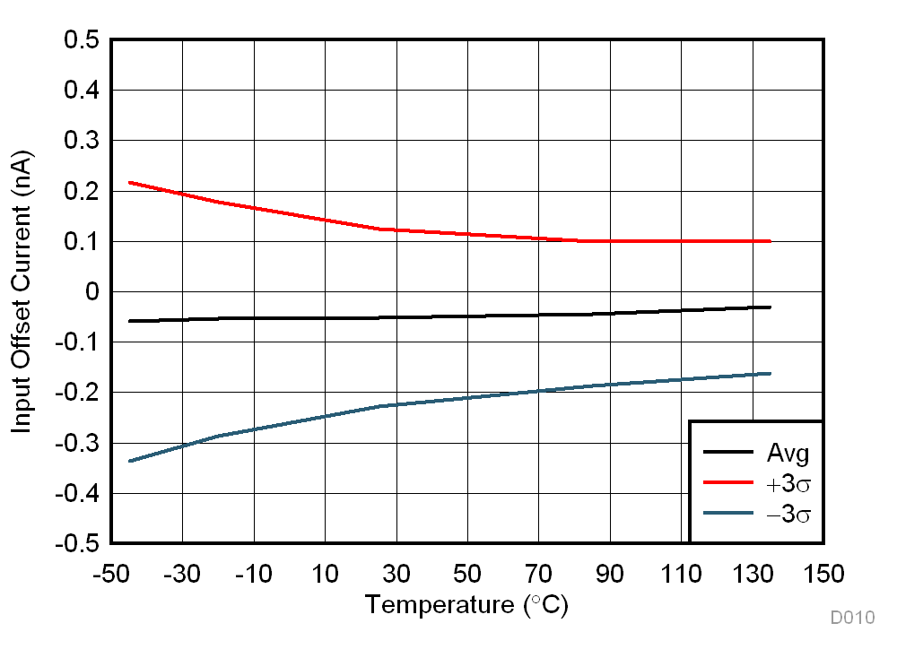
N = 294 G = 1
Figure 11. Input Offset Current vs Temperature
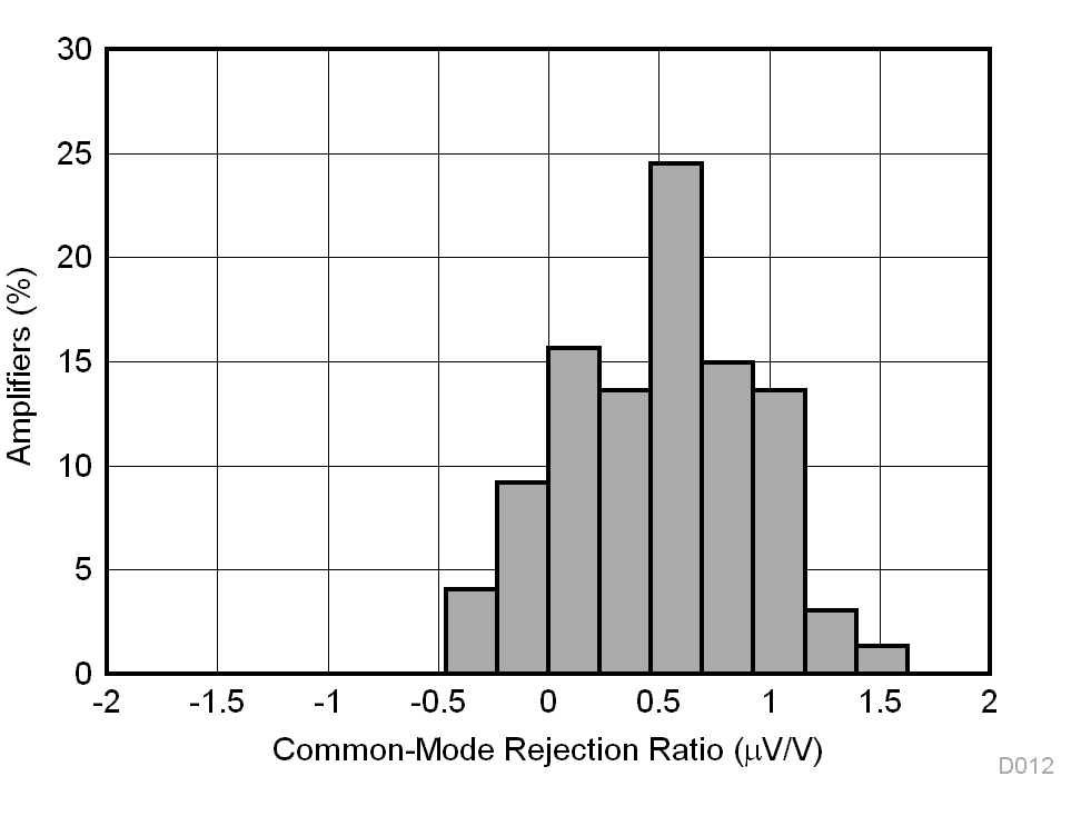
INA821 D012_INA821.gif
N = 294 Mean = 0.51 µV/V Std. Dev. = 0.42 µV/V
G = 10
Figure 13. Typical CMRR Distribution, G = 10
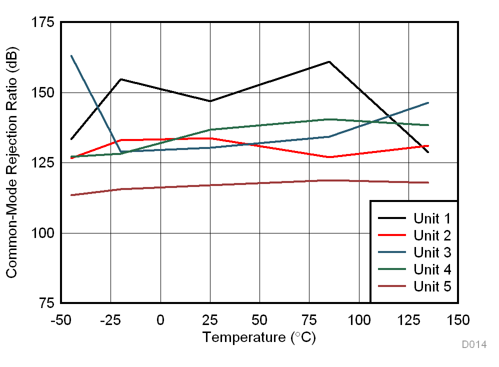
INA821 D014_INA821.gif
N = 5 G = 10
Figure 15. CMRR vs Temperature, G = 10
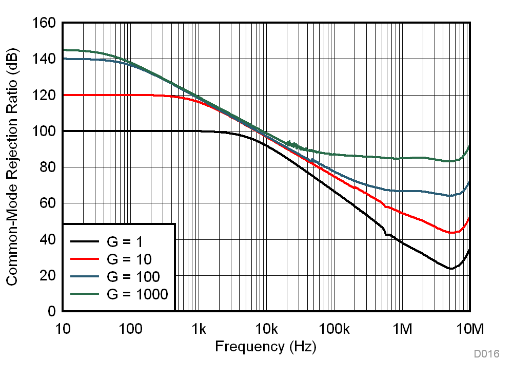
INA821 D016_INA821.gif
Figure 17. CMRR vs Frequency (RTI)
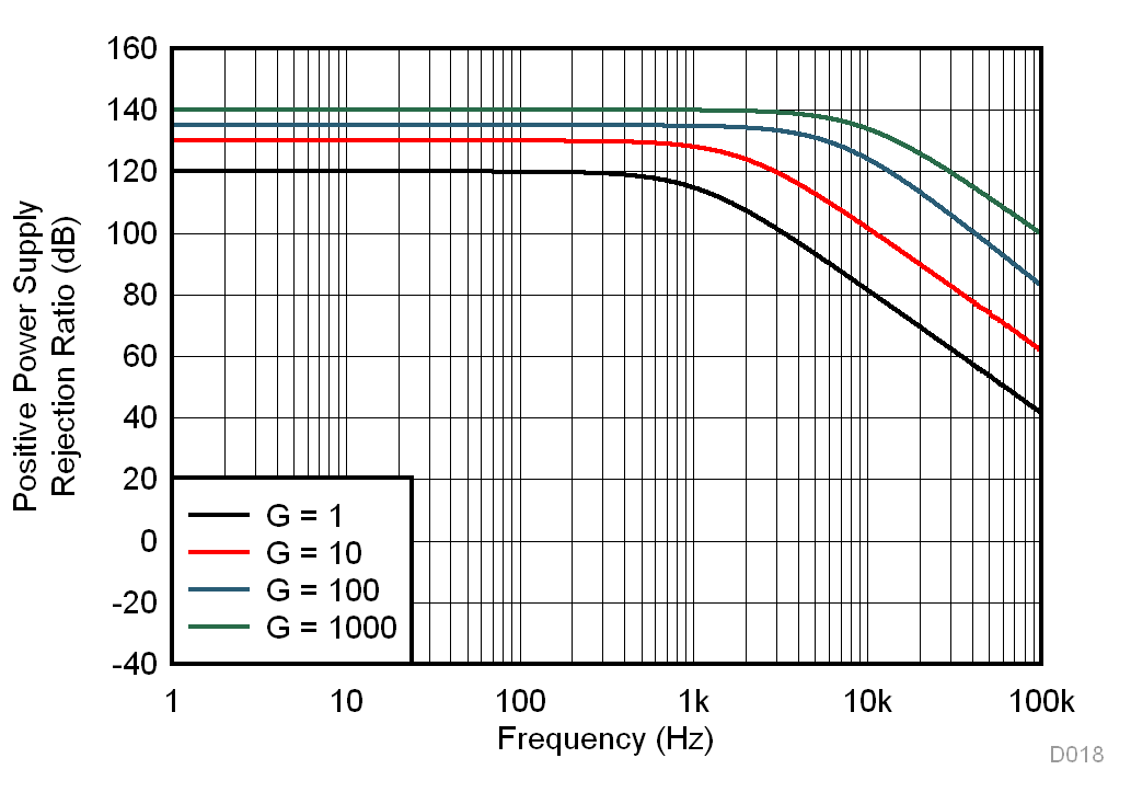
INA821 D018_INA821.gif
Figure 19. Positive PSRR vs Frequency (RTI)
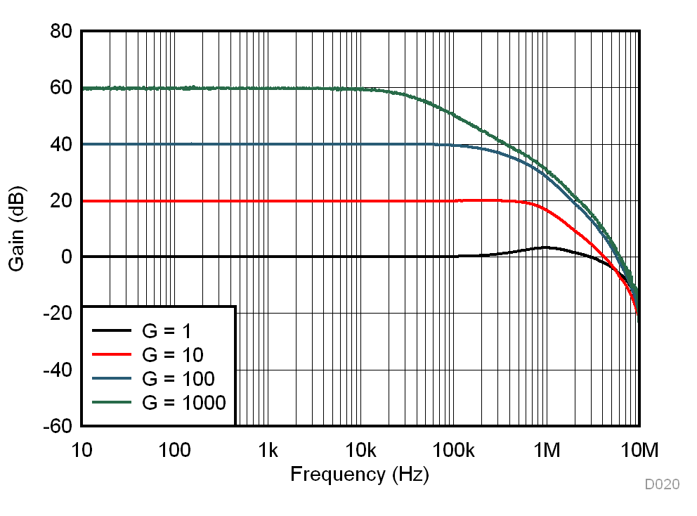
INA821 D020_INA821.gif
Figure 21. Gain vs Frequency
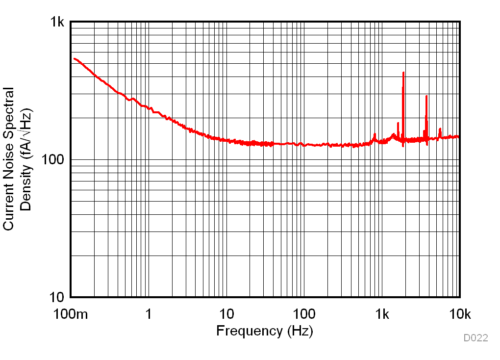
INA821 D022_INA821.gif
Figure 23. Current Noise Spectral Density vs Frequency (RTI)
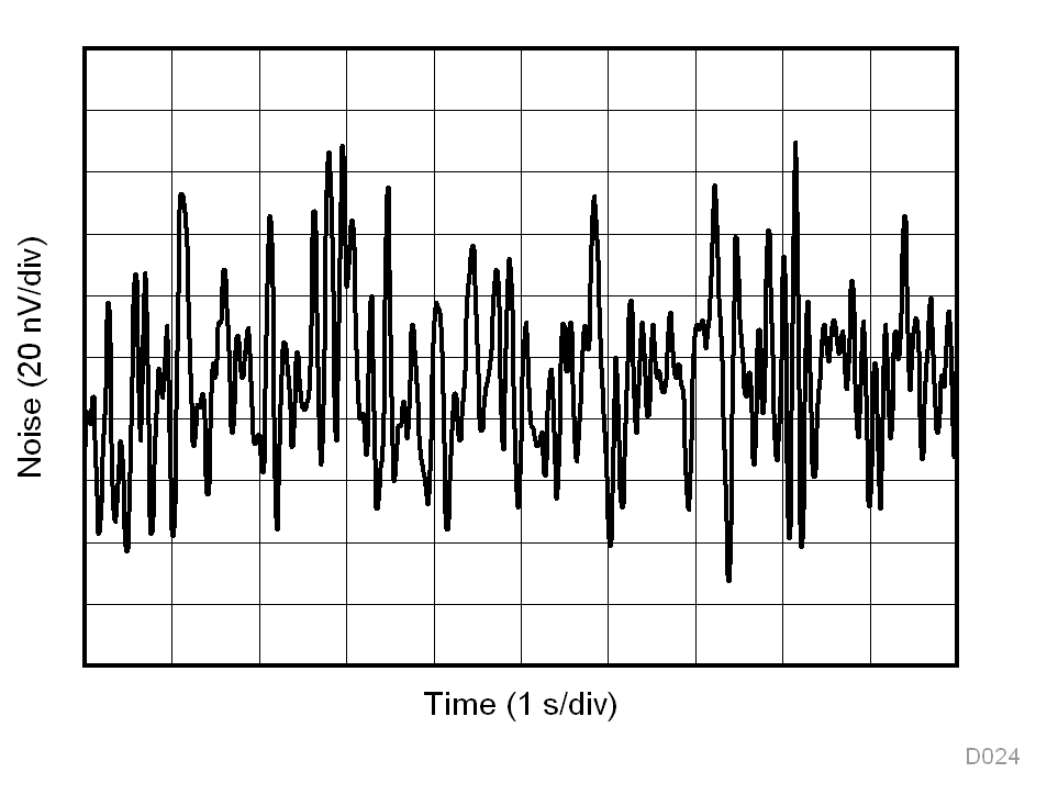
INA821 D024_INA821.gif
G = 1000
Figure 25. 0.1-Hz to 10-Hz RTI Voltage Noise, G = 1000
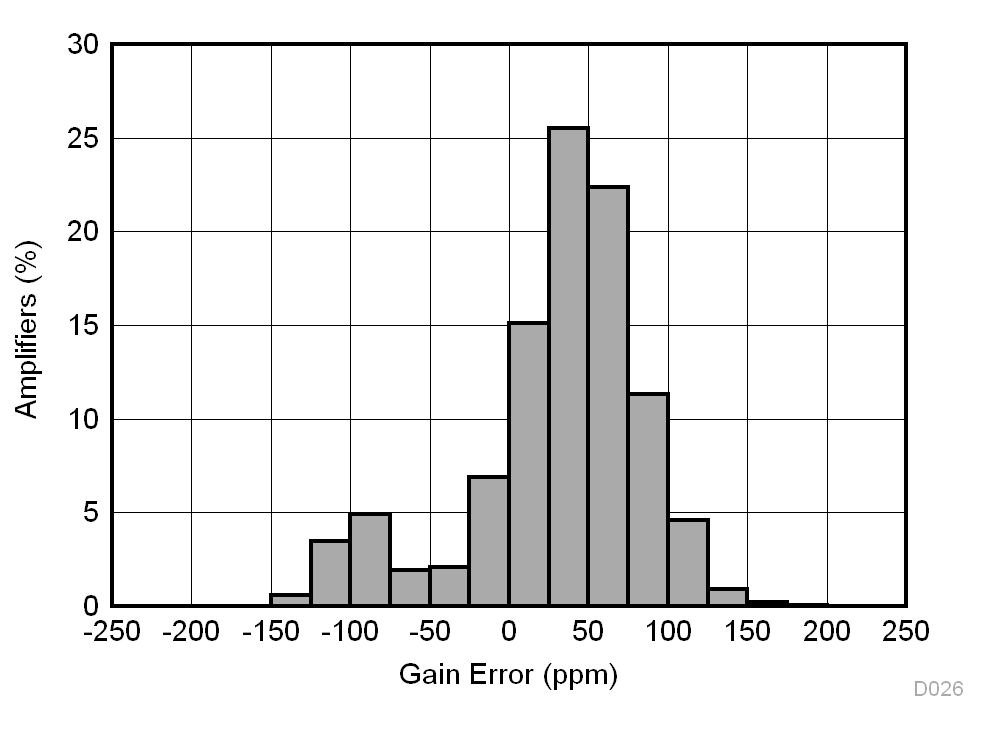
INA821 D026_INA821.gif
N = 5412 Mean = 30 ppm Std. Dev. = 55 ppm
G = 1
Figure 27. Typical Distribution of Gain Error, G = 1
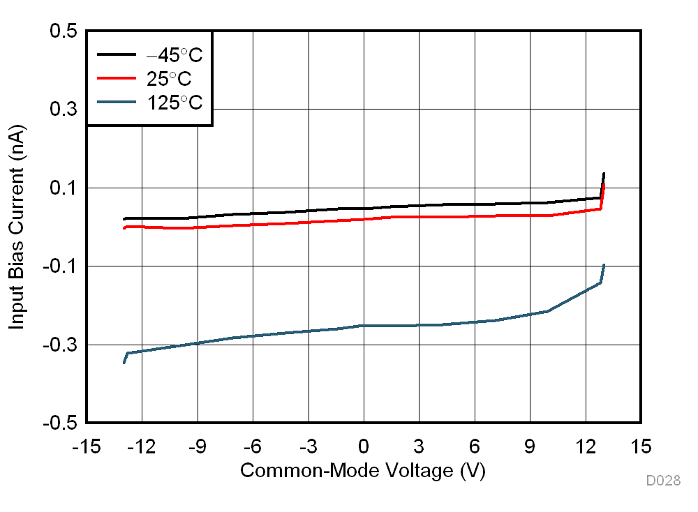
INA821 D028_INA821.gif
VS = ±15 V
Figure 29. Input Bias Current vs Common-Mode Voltage
INA821 D030_INA821.gif
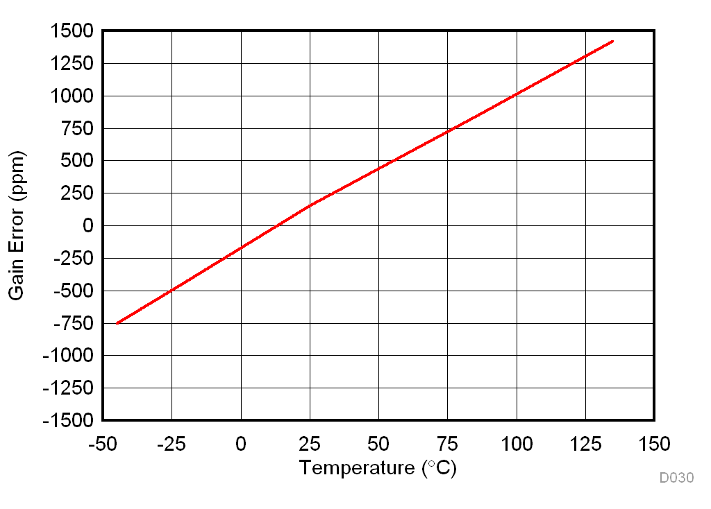
Average of 294 units G = 10
Figure 31. Gain Error vs Temperature, G = 10
INA821 D032_INA821.gif
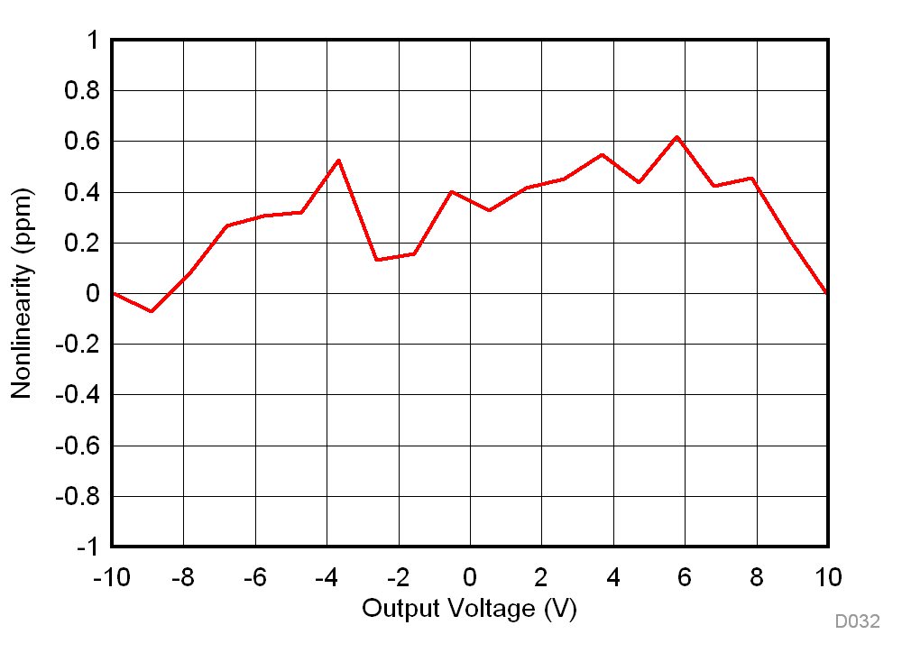
G = 1
Figure 33. Gain Nonlinearity, G = 1
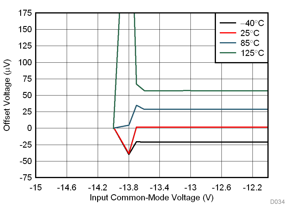
INA821 D034_INA821.gif
Figure 35. Offset Voltage vs Negative Common-Mode Voltage
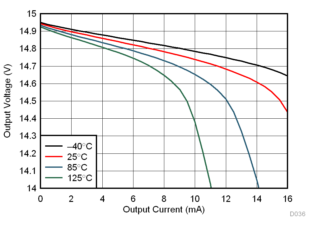
INA821 D036_INA821.gif
Figure 37. Positive Output Voltage Swing vs Output Current
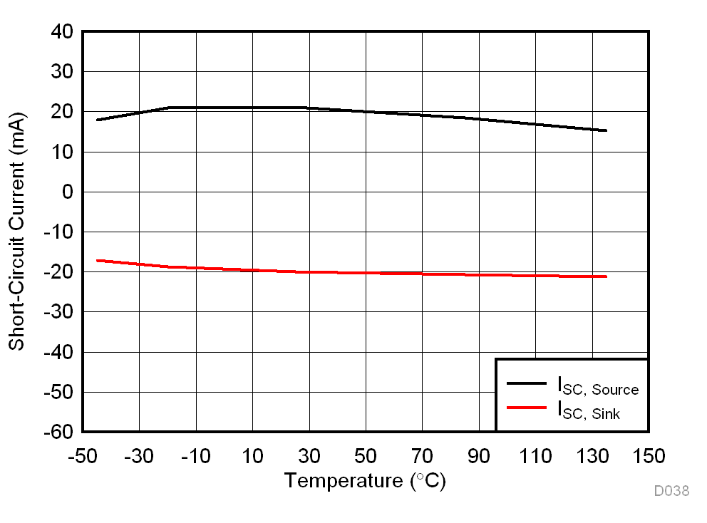
INA821 D038_INA821.gif
Figure 39. Short-Circuit Current vs Temperature
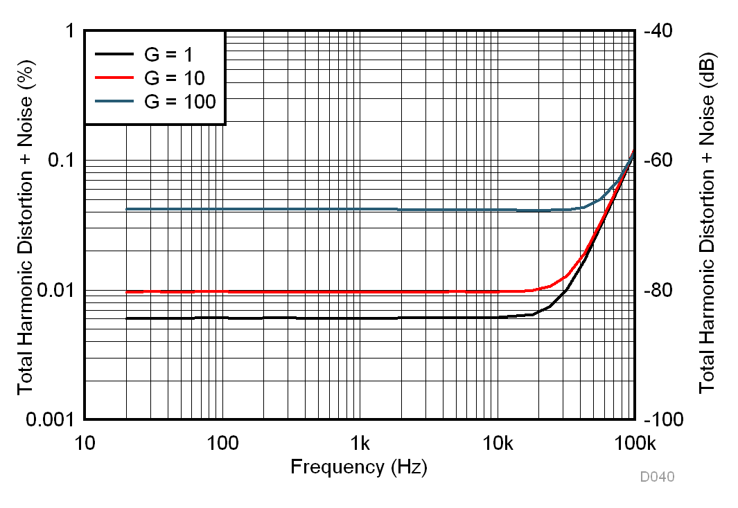
INA821 D040_INA821.gif
500-kHz measurement bandwidth
1-VRMS output voltage 100-kΩ load
Figure 41. THD+N vs Frequency
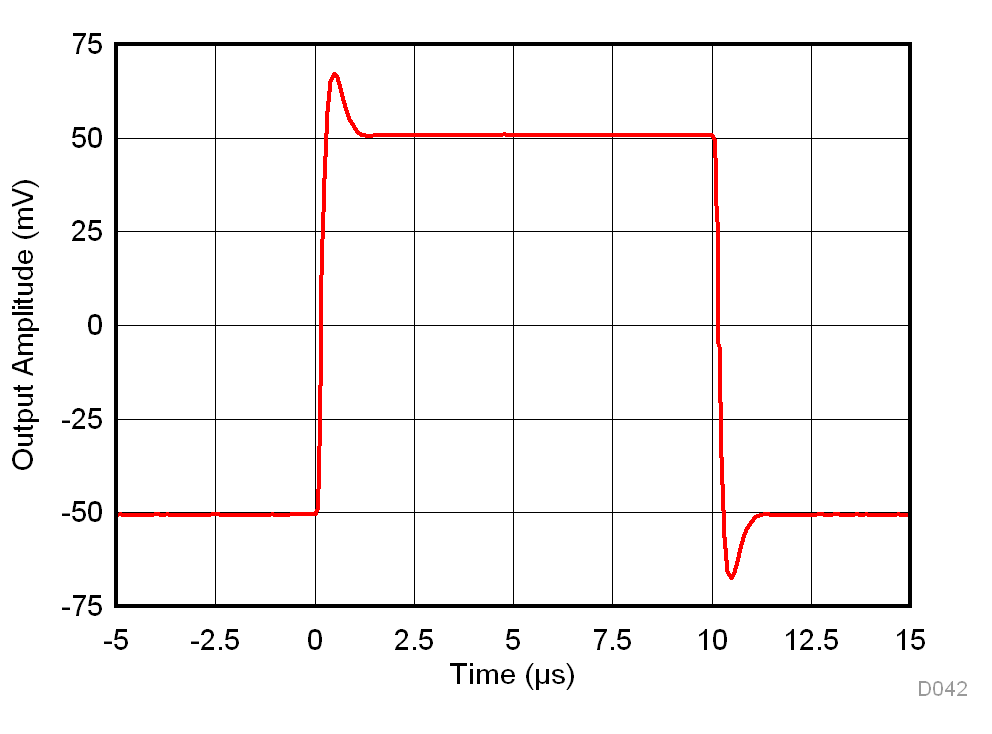
INA821 D042_INA821.gif
G = 1 RL = 10 kΩ CL = 100 pF
Figure 43. Small-Signal Response
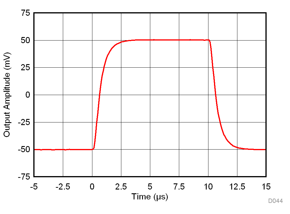
INA821 D044_INA821.gif
G = 100 RL = 10 kΩ CL = 100 pF
Figure 45. Small-Signal Response
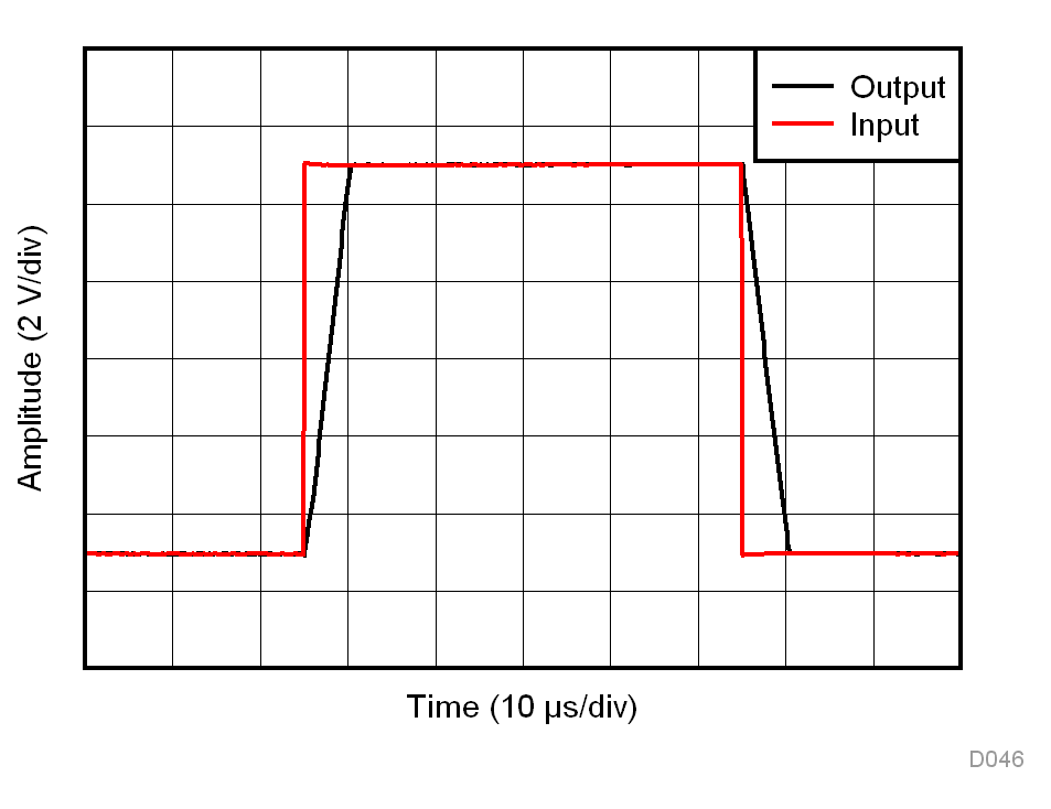
INA821 D046_INA821.gif
Figure 47. Large-Signal Step Response
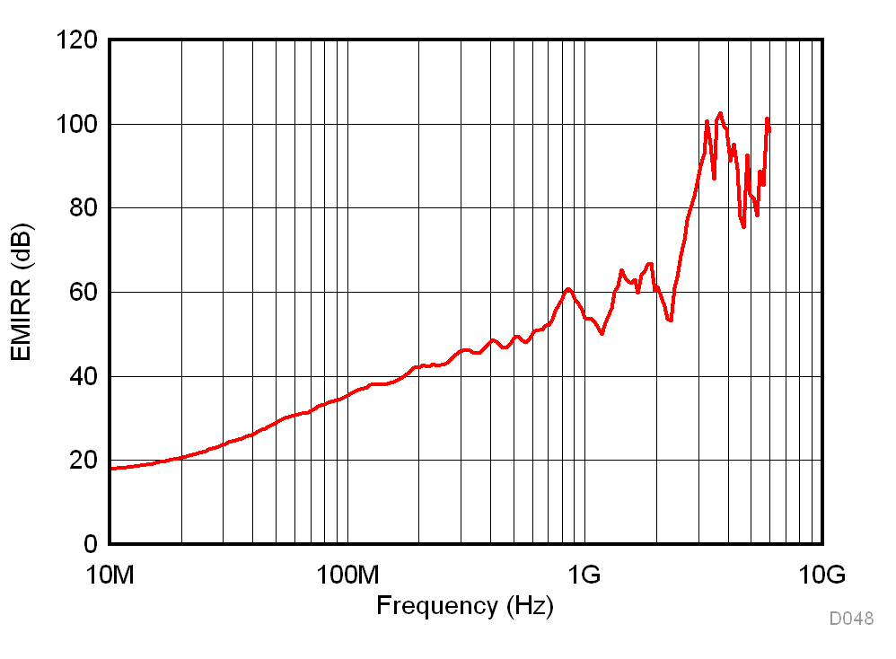
INA821 D048_INA821.gif
Figure 49. Differential-Mode EMI Rejection Ratio
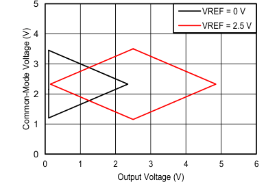
INA821 D054_SBOS959.gif
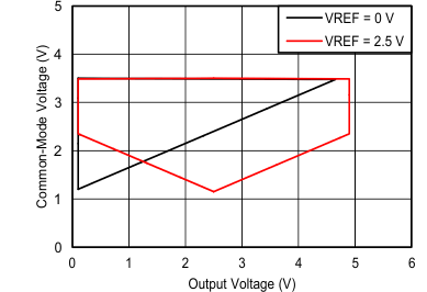
VS = 5 V G = 1
Figure 51. Input Common-Mode Voltage vs Output Voltage
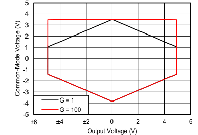
INA821 D055_SBOS959.gif
VS = ±5 V VREF = 0 V
Figure 53. Input Common-Mode Voltage vs Output Voltage
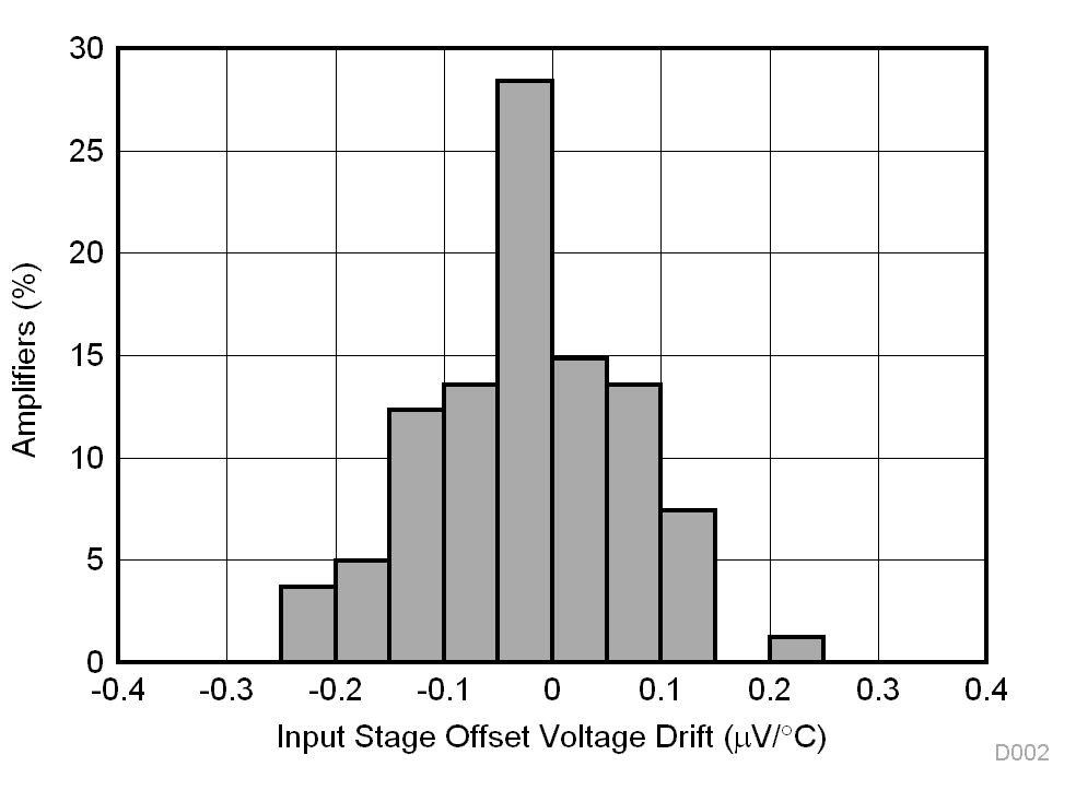
INA821 D002_INA821.gif
N = 81 Mean = -0.03 µV/°C Std. Dev. = 0.09 µV/°C
Figure 2. Typical Distribution of
Input Stage Offset Voltage Drift
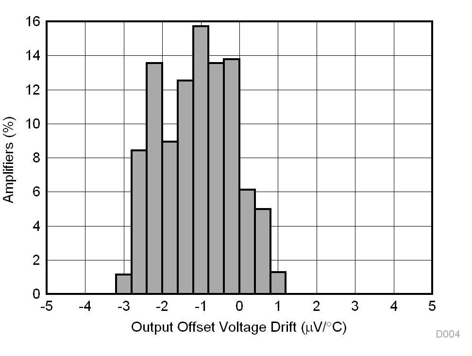
INA821 D004_INA821.gif
N = 81 Mean = –1.09 µV/°C Std. Dev. = 0.94 µV/°C
Figure 4. Typical Distribution of
Output Stage Offset Voltage Drift
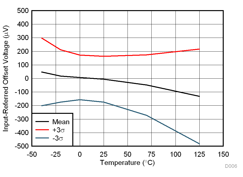
INA821 D006_INA821.gif
81 units
Figure 6. Output Stage Offset Voltage vs Temperature
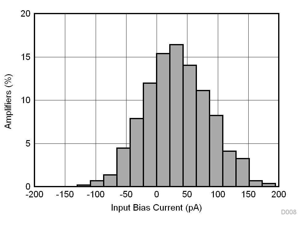
INA821 D008_INA821.gif
N = 292 Mean = 34 pA Std. Dev. = 52 pA
TA = 90°C
Figure 8. Typical Distribution of Input Bias Current,
TA = 90°C
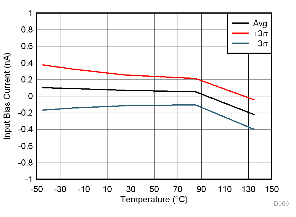
INA821 D009_INA821.gif
N = 294 G = 1
Figure 10. Input Bias Current vs Temperature
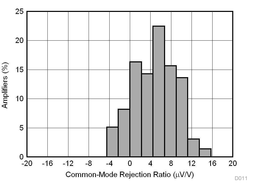
INA821 D011_INA821.gif
N = 294 Mean = 4.87 µV/V Std. Dev. = 4.14 µV/V
G = 1
Figure 12. Typical CMRR Distribution, G = 1
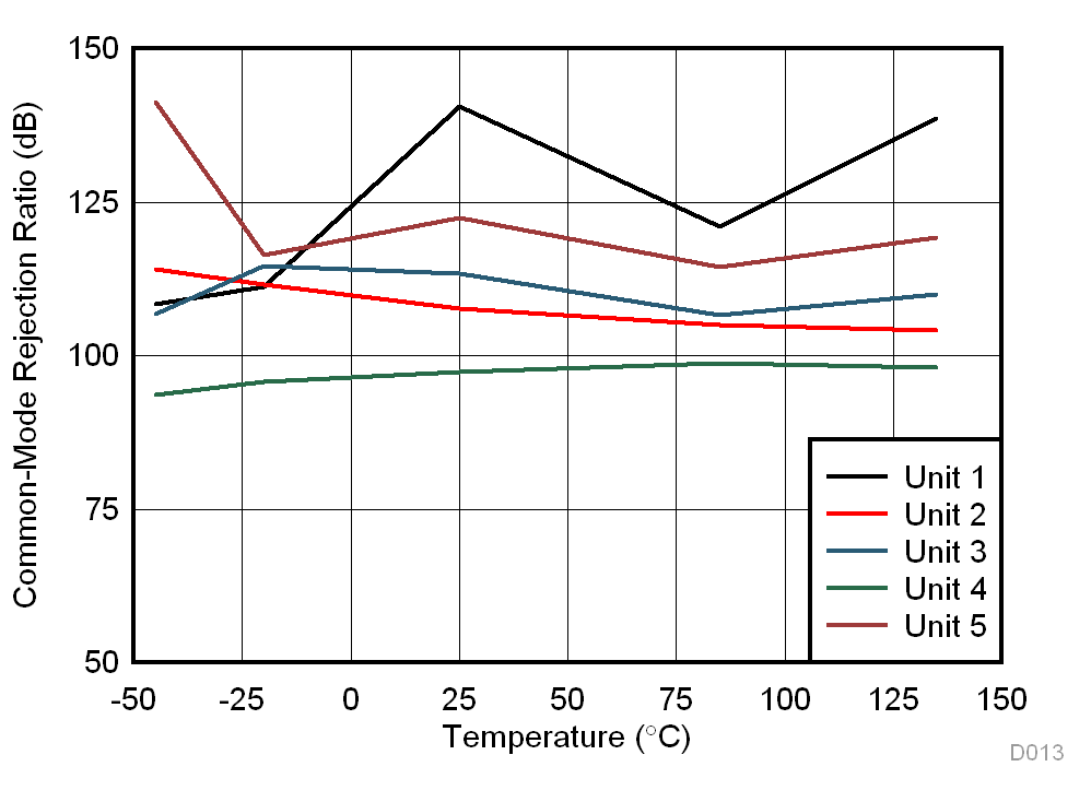
INA821 D013_INA821.gif
N = 5 G = 1
Figure 14. CMRR vs Temperature, G = 1
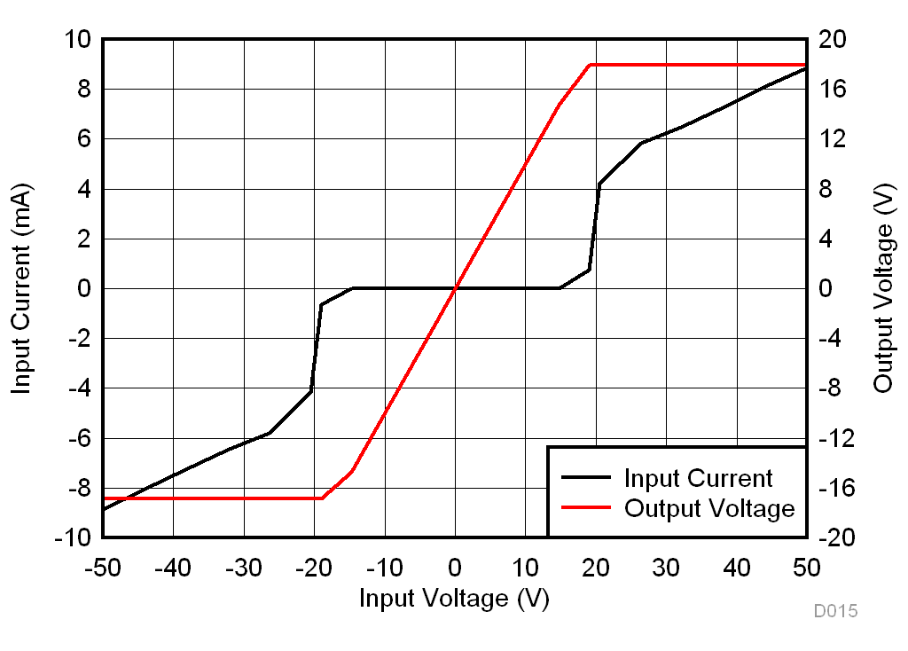
INA821 D015_INA821.gif
VS = ±18 V
Figure 16. Input Current vs Input Overvoltage
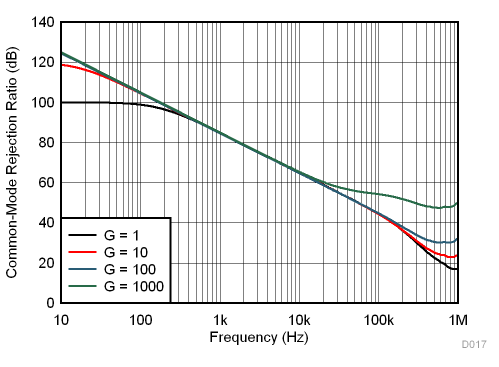
INA821 D017_INA821.gif
Figure 18. CMRR vs Frequency
(RTI, 1-kΩ source imbalance)
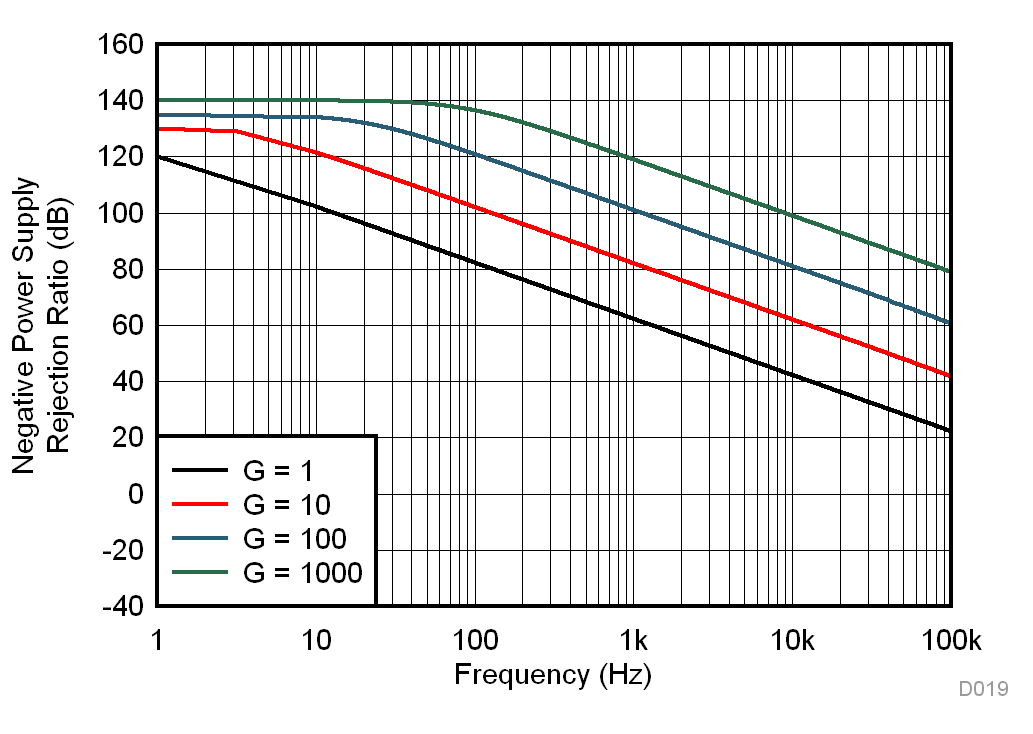
INA821 D019_INA821.gif
Figure 20. Negative PSRR vs Frequency (RTI)
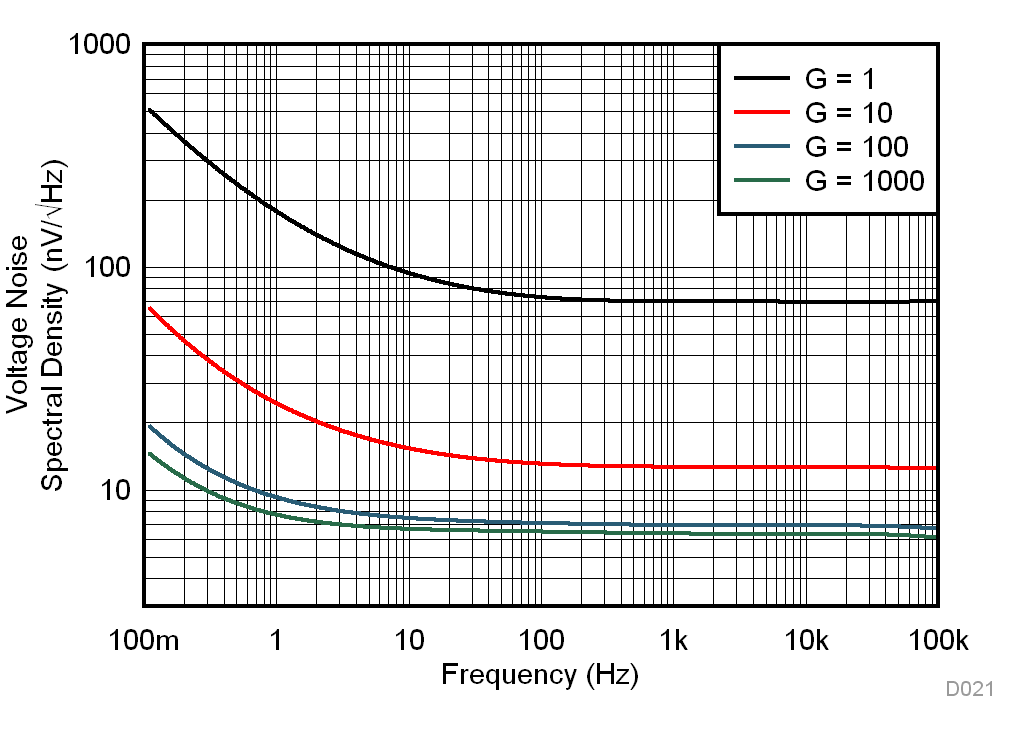
INA821 D021_INA821.gif
Figure 22. Voltage Noise Spectral Density vs Frequency (RTI)
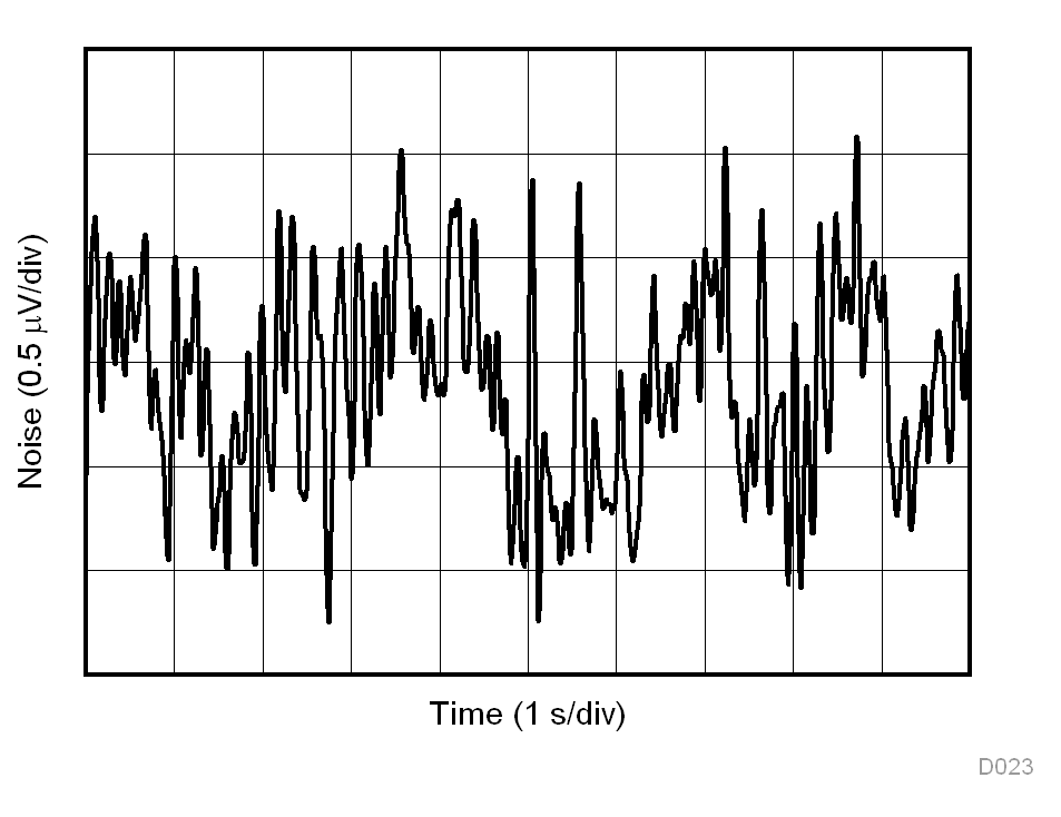
INA821 D023_INA821.gif
G = 1
Figure 24. 0.1-Hz to 10-Hz RTI Voltage Noise, G = 1
INA821 D025_INA821.gif
G = 1
Figure 26. 0.1-Hz to 10-Hz RTI Current Noise
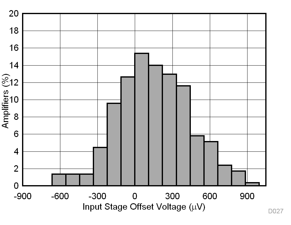
INA821 D027_INA821.gif
N = 293 Mean = 152 ppm Std. Dev. = 291 ppm
G = 10
Figure 28. Typical Distribution of Gain Error, G = 10
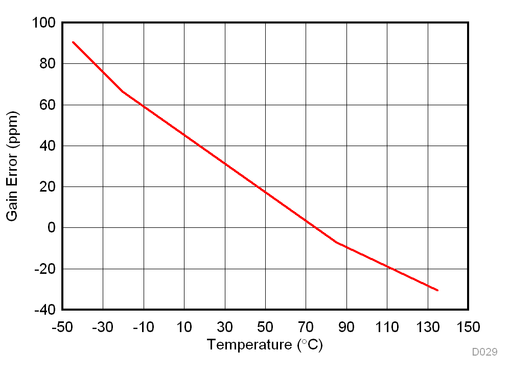
INA821 D029_INA821.gif
Average of 294 units G = 1
Figure 30. Gain Error vs Temperature, G = 1
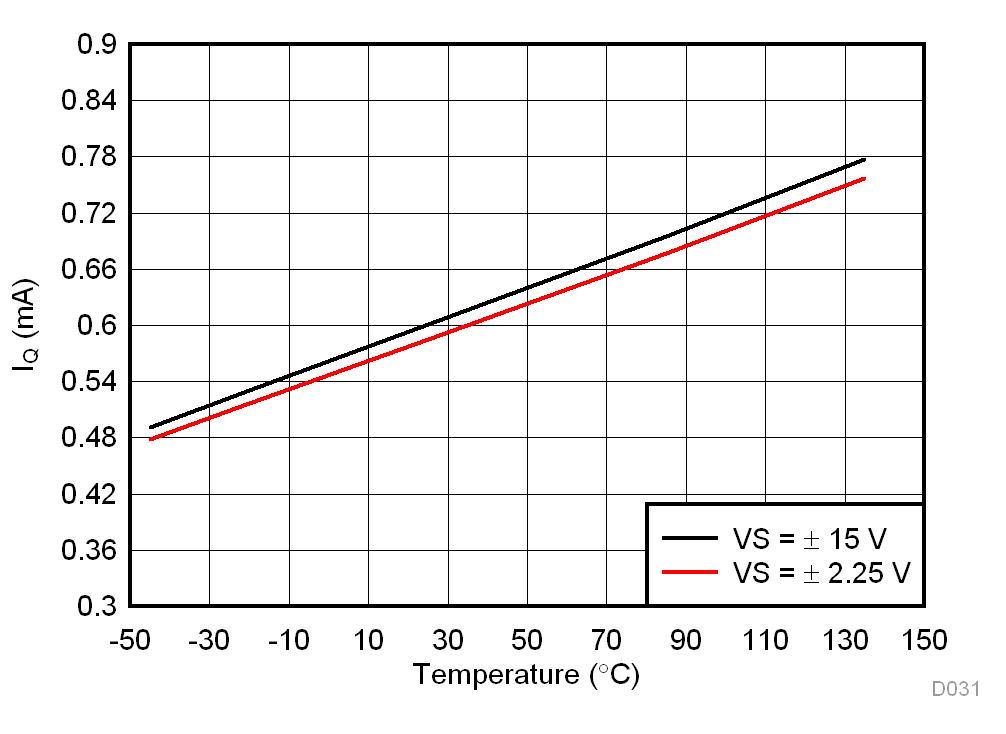
INA821 D031_INA821.gif
Figure 32. Supply Current vs Temperature
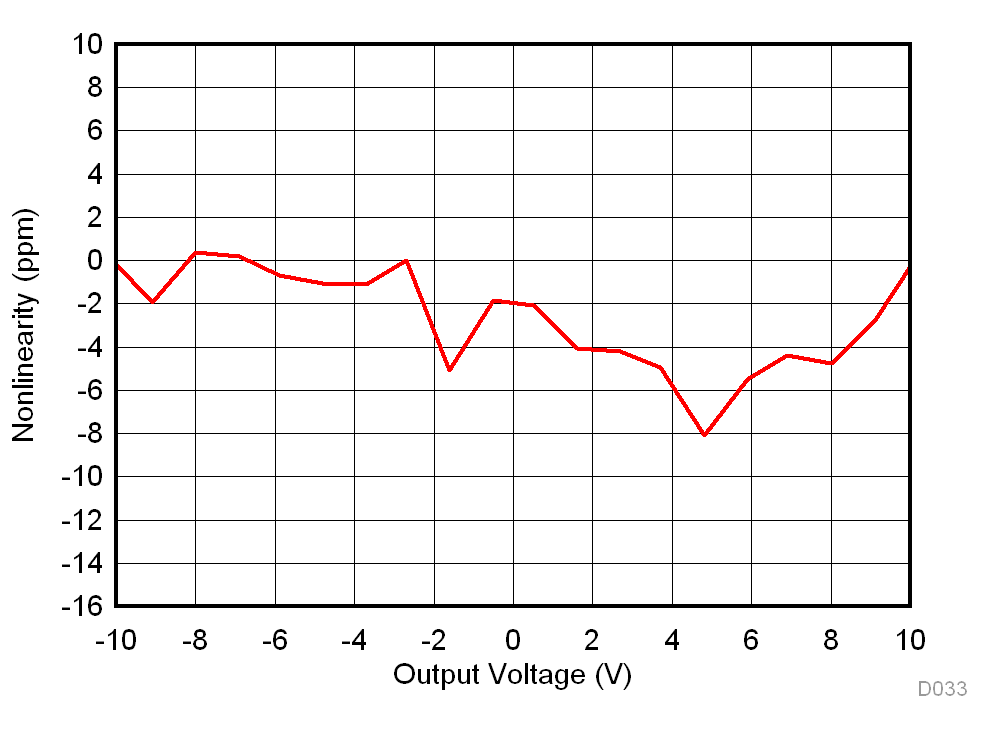
INA821 D033_INA821.gif
G = 10
Figure 34. Gain Nonlinearity, G = 10
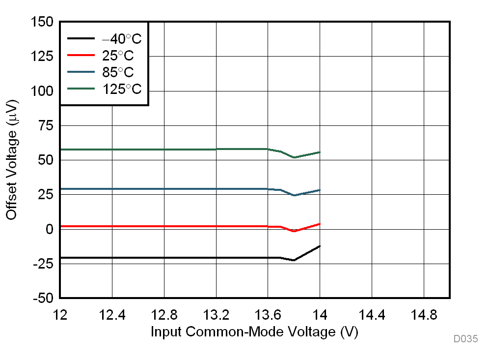
INA821 D035_INA821.gif
Figure 36. Offset Voltage vs Positive Common-Mode Voltage
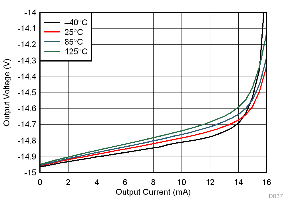
INA821 D037_INA821.gif
Figure 38. Negative Output Voltage Swing vs Output Current
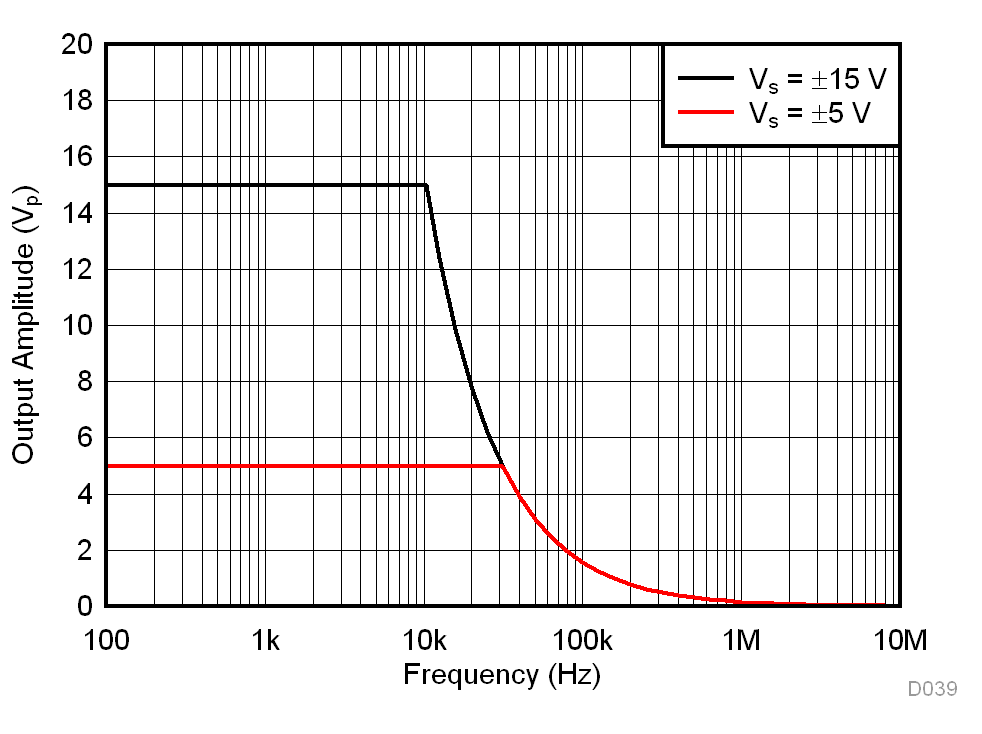
INA821 D039_INA821.gif
Figure 40. Large-Signal Frequency Response
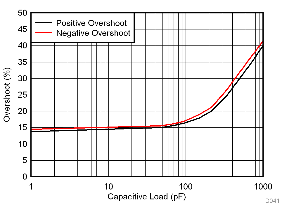
INA821 D041_INA821.gif
Figure 42. Overshoot vs Capacitive Loads
INA821 D043_INA821.gif
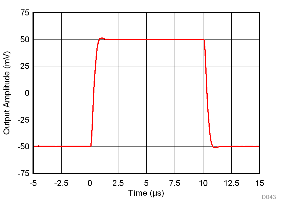
G = 10 RL = 10 kΩ CL = 100 pF
Figure 44. Small-Signal Response
INA821 D045_INA821.gif
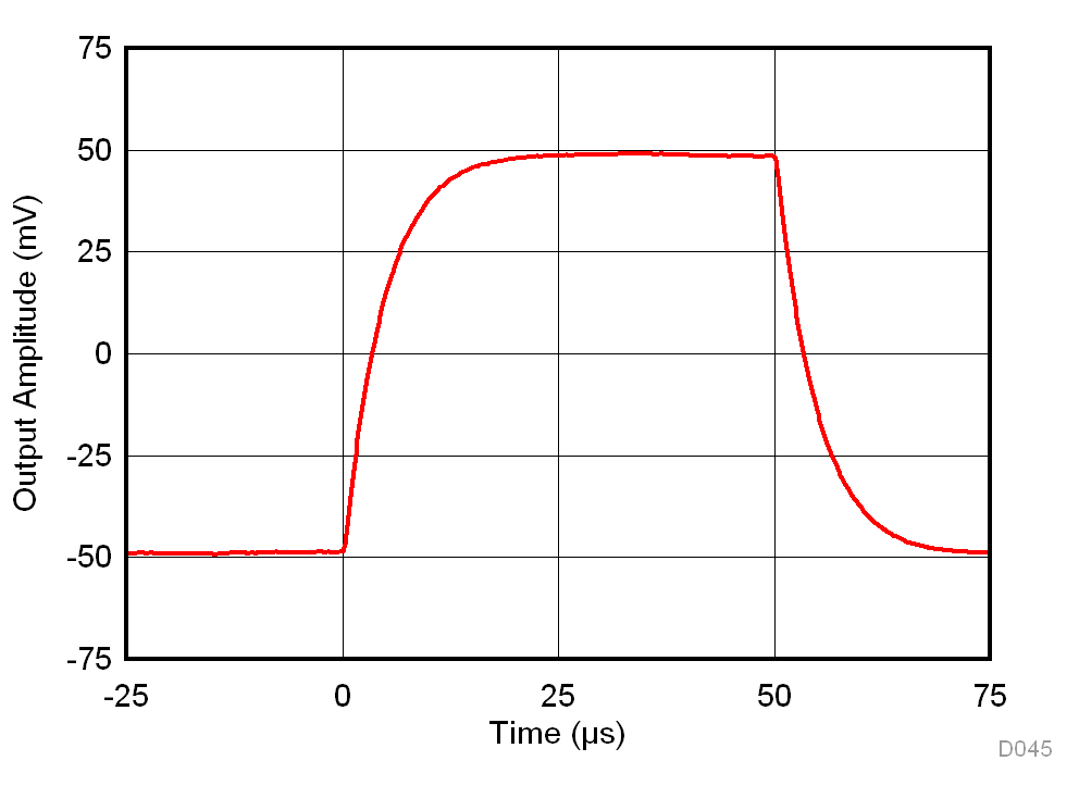
G = 1000 RL = 10 kΩ CL = 100 pF
Figure 46. Small-Signal Response
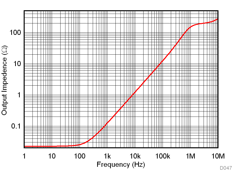
INA821 D047_INA821.gif
Figure 48. Closed-Loop Output Impedance
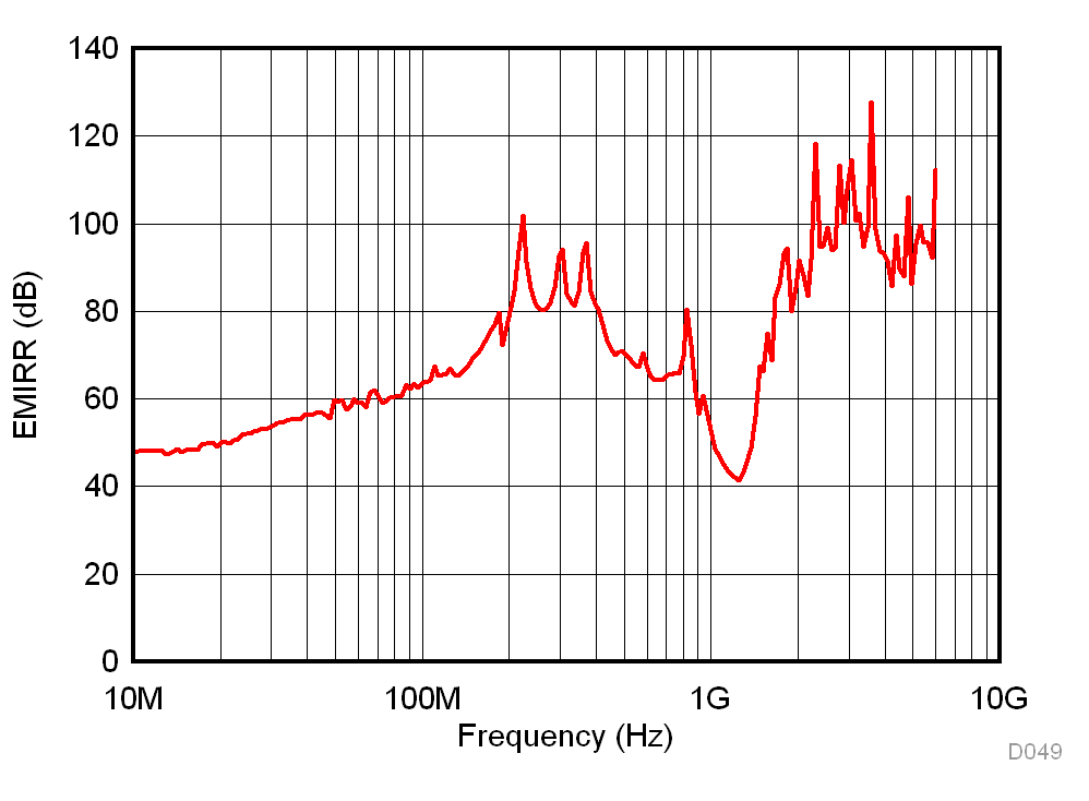
INA821 D049_INA821.gif
Figure 50. Common-Mode EMI Rejection Ratio
INA821 D056_SBOS959.gif
VS = 5 V G = 100
Figure 52. Input Common-Mode Voltage vs Output Voltage
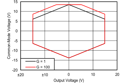
INA821 D052_SBOS959.gif
VS = ±15 V VREF = 0 V
Figure 54. Input Common-Mode Voltage vs Output Voltage