ZHCSIM8C August 2018 – July 2019 INA821
PRODUCTION DATA.
- 1 特性
- 2 应用
- 3 说明
- 4 修订历史记录
- 5 Device Comparison Table
- 6 Pin Configuration and Functions
- 7 Specifications
- 8 Detailed Description
- 9 Application and Implementation
- 10Power Supply Recommendations
- 11Layout
- 12器件和文档支持
- 13机械、封装和可订购信息
封装选项
机械数据 (封装 | 引脚)
散热焊盘机械数据 (封装 | 引脚)
- DRG|8
订购信息
8.3.4 Input Protection
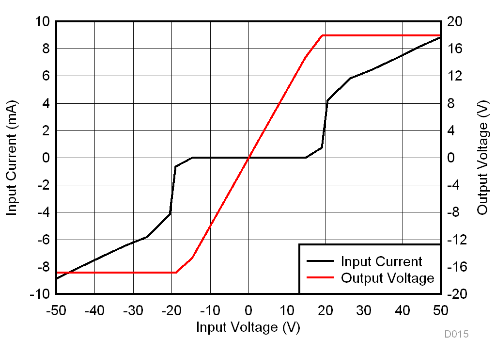
The inputs of the INA821 device are individually protected for voltages up to ±40 V. For example, a condition of –40 V on one input and +40 V on the other input does not cause damage. Internal circuitry on each input provides low series impedance under normal signal conditions. If the input is overloaded, the protection circuitry limits the input current to a value of approximately 8 mA.
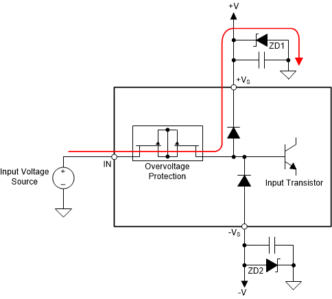
 Figure 62. Input Current Path During an Overvoltage Condition
 During an input overvoltage condition, current flows through the input protection diodes into the power supplies; see Figure 62. If the power supplies are unable to sink current, then Zener diode clamps (ZD1 and ZD2 in Figure 62) must be placed on the power supplies to provide a current pathway to ground. Figure 63 shows the input current for input voltages from –40 V to 40 V when the INA821 is powered by ±15-V supplies.
 Figure 63. Input Current vs Input Overvoltage