ZHCSNH8B July 2021 – November 2021 INA823
PRODUCTION DATA
- 1 特性
- 2 应用
- 3 说明
- 4 Revision History
- 5 Device Comparison Table
- 6 Pin Configuration and Functions
- 7 Specifications
- 8 Detailed Description
- 9 Application and Implementation
- 10Power Supply Recommendations
- 11Layout
- 12Device and Documentation Support
- 13Mechanical, Packaging, and Orderable Information
8.3.2 Input Common-Mode Voltage Range
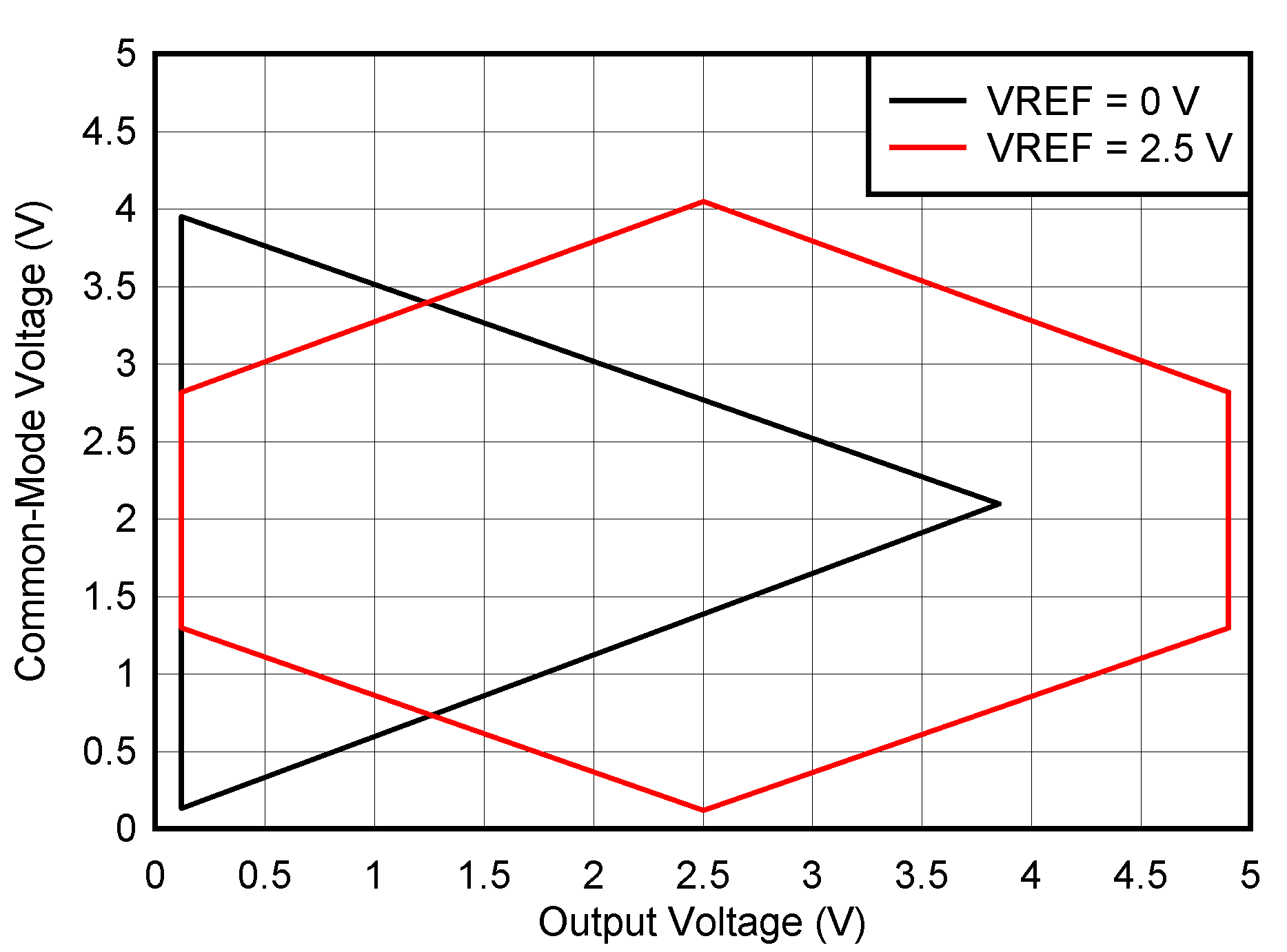
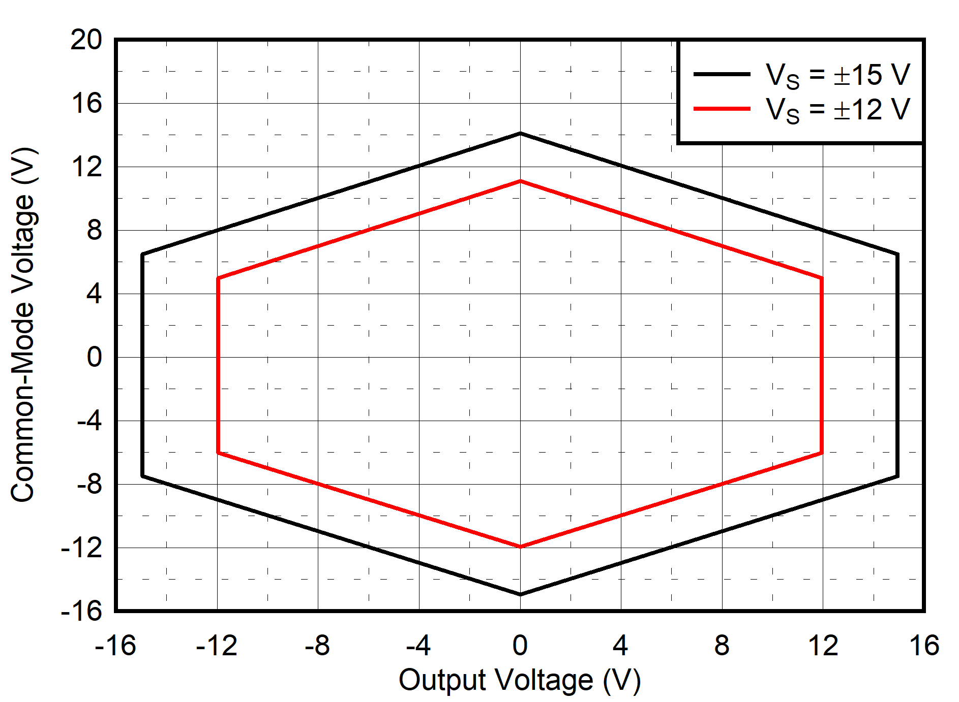
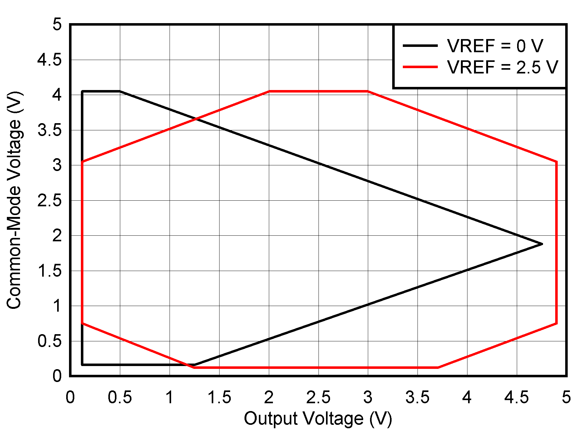
The INA823 linear input voltage range extends from 1 V less than the positive supply to 0.15 V less than the negative supply, and maintains excellent common-mode rejection throughout this range. The common-mode range for the most common operating conditions are shown in Figure 8-3. While there are other methods to calculate the common-mode voltage range, the suggested tool is the Analog Engineers Calculator.

| VS = 5 V, G = 1 |

| G = 1, VREF = 0 V |

| VS = 5 V, G = 100 |

| G > 10, VREF = 0 V |
A single-supply instrumentation amplifier has special design considerations. To achieve a common-mode range that extends to single-supply ground, the INA823 employs a current-feedback topology with PNP input transistors. The matched PNP transistors, Q1 and Q2, shift the input voltages of both inputs up by a diode drop, and (through the feedback network) shift the output of A1 and A2 by approximately 0.6 V. The output of A1 and A2 is well within the linear range when the inputs are within the single-supply ground. When inputs are within the supply ground, differential measurements can be made at the ground level. As a result of this input level-shifting, the voltages at pin 1 and pin 8 are not equal to the respective input pin voltages. For most applications, this inequality is not important because only the gain-setting resistor connects to these pins.