ZHCSGB6A May 2017 – June 2017 INA826S
PRODUCTION DATA.
8 Application and Implementation
NOTE
Information in the following applications sections is not part of the TI component specification, and TI does not warrant its accuracy or completeness. TI’s customers are responsible for determining suitability of components for their purposes. Customers should validate and test their design implementation to confirm system functionality.
8.1 Application Information
The low power consumption and high performance of the INA826S make the device an excellent instrumentation amplifier for many applications. The INA826S can be used in many low-power, portable applications because the device has a low quiescent current (200 µA, typical) and comes in a small 10-pin VSON package. The input protection circuitry, low maximum gain drift, low offset voltage, and 36-V maximum supply voltage also make the INA826S an ideal choice for industrial applications as well.
8.2 Typical Application
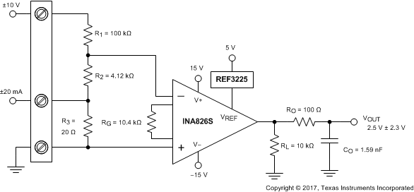
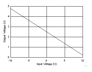
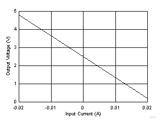
Figure 74 shows a three-terminal, programmable-logic controller (PLC) design for the INA826S. This PLC reference design accepts inputs of ±10 V or ±20 mA. The output is a single-ended voltage of 2.5 V ± 2.3 V (or 200 mV to 4.8 V). Many PLCs typically have these input and output ranges.
 Figure 74. Three-Terminal Analog Input for PLCs
8.2.1 Design Requirements
This design has the following requirements:
- Supply voltage: ±15 V, 5 V
- Inputs: ±10 V, ±20 mA
- Output: 2.5 V, ±2.3 V
8.2.2 Detailed Design Procedure
There are two modes of operation for the circuit shown in Figure 74: current input and voltage input. This design requires R1 >> R2 >> R3. Given this relationship, Equation 2 calculates the current input mode transfer function.

where
- G represents the gain of the instrumentation amplifier
Equation 3 shows the transfer function for the voltage input mode.

R1 sets the input impedance of the voltage input mode. The minimum typical input impedance is 100 kΩ. 100 kΩ is selected for R1 because increasing the R1 value also increases noise. The value of R3 must be extremely small compared to R1 and R2. 20 Ω for R3 is selected because that resistance value is much smaller than R1 and yields an input voltage of ±400 mV when operated in current mode (±20 mA).
Equation 4 can be used to calculate R2 given VD = ±400 mV, VIN = ±10 V, and R1 = 100 kΩ.

The value obtained from Equation 4 is not a standard 0.1% value, so 4.12 kΩ is selected. R1 and R2 also use 0.1% tolerance resistors to minimize error.
Use Equation 5 to calculate the ideal gain of the instrumentation amplifier.

Equation 6 calculates the gain-setting resistor value using the INA826S gain equation, Equation 1.

10.4 kΩ is a standard 0.1% resistor value that can be used in this design. Finally, the output RC filter components are selected to have a –3-dB cutoff frequency of 1 MHz.

