ZHCS968B June 2012 – November 2017 INA827
PRODUCTION DATA.
- 1 特性
- 2 应用
- 3 说明
- 4 修订历史记录
- 5 Pin Configuration and Functions
- 6 Specifications
- 7 Typical Characteristics
- 8 Detailed Description
- 9 Application and Implementation
- 10Power Supply Recommendations
- 11Layout
- 12器件和文档支持
- 13机械、封装和可订购信息
8.3.4 Inside the INA827
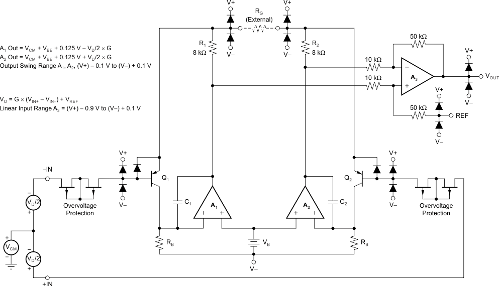
See Figure 61 for a simplified representation of the INA827. A more detailed diagram (shown in Figure 57) provides additional insight into the INA827 operation.
Each input is protected by two field-effect transistors (FETs) that provide a low series resistance under normal signal conditions and preserve excellent noise performance. When excessive voltage is applied, these transistors limit input current to approximately 8 mA.
The differential input voltage is buffered by Q1 and Q2 and is applied across RG, causing a signal current to flow through RG, R1, and R2. The output difference amplifier (A3) removes the common-mode component of the input signal and refers the output signal to the REF pin.
The equations shown in Figure 57 describe the output voltages of A1 and A2. The VBE and voltage drop across R1 and R2 produce output voltages on A1 and A2 that are approximately 0.8 V higher than the input voltages.
 Figure 57. INA827 Simplified Circuit Diagram