ZHCS968B June   2012  – November 2017 INA827

PRODUCTION DATA.  

  1. 特性
  2. 应用
  3. 说明
    1.     简化电路原理图
  4. 修订历史记录
  5. Pin Configuration and Functions
    1.     Pin Functions
  6. Specifications
    1. 6.1 Absolute Maximum Ratings
    2. 6.2 ESD Ratings
    3. 6.3 Recommended Operating Conditions
    4. 6.4 Thermal Information
    5. 6.5 Electrical Characteristics
  7. Typical Characteristics
  8. Detailed Description
    1. 8.1 Overview
    2. 8.2 Functional Block Diagram
    3. 8.3 Feature Description
      1. 8.3.1  Setting the Gain
        1. 8.3.1.1 Gain Drift
      2. 8.3.2  Offset Trimming
      3. 8.3.3  Input Common-Mode Range
      4. 8.3.4  Inside the INA827
      5. 8.3.5  Input Protection
      6. 8.3.6  Input Bias Current Return Path
      7. 8.3.7  Reference Pin
      8. 8.3.8  Dynamic Performance
      9. 8.3.9  Operating Voltage
        1. 8.3.9.1 Low-Voltage Operation
      10. 8.3.10 Error Sources
    4. 8.4 Device Functional Modes
  9. Application and Implementation
    1. 9.1 Application Information
    2. 9.2 Typical Application
      1. 9.2.1 Design Requirements
      2. 9.2.2 Detailed Design Procedure
      3. 9.2.3 Application Curves
  10. 10Power Supply Recommendations
  11. 11Layout
    1. 11.1 Layout Guidelines
      1. 11.1.1 CMRR vs Frequency
    2. 11.2 Layout Example
  12. 12器件和文档支持
    1. 12.1 文档支持
      1. 12.1.1 相关文档
    2. 12.2 接收文档更新通知
    3. 12.3 社区资源
    4. 12.4 商标
    5. 12.5 静电放电警告
    6. 12.6 Glossary
  13. 13机械、封装和可订购信息

封装选项

机械数据 (封装 | 引脚)
散热焊盘机械数据 (封装 | 引脚)
订购信息

Application Information

Figure 61 shows the basic connections required for device operation. Good layout practice mandates that bypass capacitors are placed as close to the device pins as possible.

The INA827 output is referred to the output reference (REF) pin, which is normally grounded. This connection must be low-impedance to assure good common-mode rejection. Although 5 Ω or less of stray resistance can be tolerated when maintaining specified CMRR, small stray resistances of tens of ohms in series with the REF pin can cause noticeable degradation in CMRR.
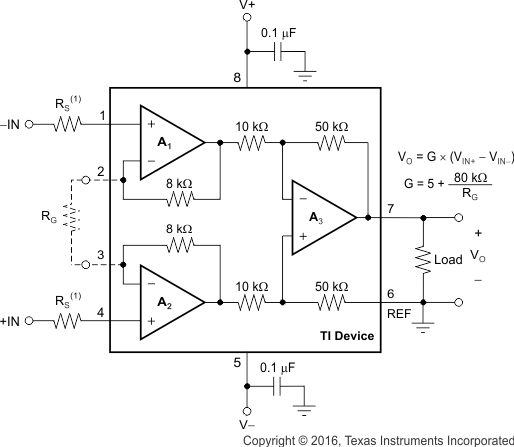
INA827 ai_basic_connex_bos631.gif

NOINDENT:

This resistor is optional if the input voltage remains above [(V–) – 2 V] or if the signal source current drive capability is limited to less than 3.5 mA. See the Input Protection section for more details.
Figure 61. Basic Connections