ZHCSOW3 September 2020 INA848
PRODUCTION DATA
- 1 特性
- 2 应用
- 3 说明
- 4 Revision History
- 5 Device Comparison Table
- 6 Pin Configuration and Functions
- 7 Specifications
- 8 Detailed Description
- 9 Application and Implementation
- 10Power Supply Recommendations
- 11Layout
- 12Device and Documentation Support
- 13Mechanical, Packaging, and Orderable Information
9.2.2.1 Reference Pin
The output voltage of the INA848 is developed with respect to the voltage on the reference pin (REF.)
The voltage source applied to the reference pin of the INA848 must have a low output impedance (RREF > 5 Ω). Any additional resistance at the reference pin creates an imbalance in the four resistors of the internal difference amplifier, resulting in degraded common-mode rejection ratio (CMRR).
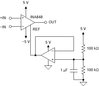
Voltage reference devices are an excellent option for providing a low-impedance voltage source for the reference pin. However, if a resistor voltage divider generates a reference voltage, the divider must be buffered by an op amp, as shown in Figure 9-5, to avoid CMRR degradation.
 Figure 9-5 Buffer to drive
the Reference Voltage
Figure 9-5 Buffer to drive
the Reference VoltageOften in dual-supply operation, the reference pin connects to the low-impedance system ground. The degradation effect of common-mode rejection ratio is thus neglegible as long as the output voltage (VOUT) is referred to the reference pin (REF).
In single-supply operation, the output signal is offset to a precise midsupply level (for example, 2.5 V in a 5-V supply environment). In applications where the output voltage is offset to a reference voltage but referred to system ground, the degradation effect of common-mode rejection ratio must be considered.