Table 9-4 and Table 9-5 show the typical signal-to-noise (SNR) and total harmonic distortion (THD) of the
INA851 driving the ADS127L11 delta-sigma ADC at full-scale range and at different
gain configurations.
The RC filter combination is
dimensioned such to help attenuate the nonlinear charge kickback and optimize for
best THD performance. The ADC requires a low impedance input for lowest distortion
performance; however, driving heavier loads degrades the phase margin of the INA851.
Use a feedback capacitor (CFB) in the range of 47 pF to 100 pF to
optimize for stability versus THD performance. Low voltage-coefficient C0G
capacitors are used everywhere in the signal path (CFB, CDIFF,
CCM) for their low distortion properties.
For other bandwidth requirements,
adjust the feedback capacitor accordingly and verify the circuit performance using a
SPICE simulation using INA851 TINA-TI™ SPICE Model. Confirm that the desired
circuit is stable; that is, the FDA has more than a 45º phase margin.
(1) Used 1 × input range for best THD. All other cases use 2 ×
input range.
Table 9-4 INA851 + ADS127L11 (Sinc4
Filter) FFT Data Summary
| INPUT
AMPLITUDE (Vpk) |
RG RESISTOR
(Ω) |
GIN (V/V) |
GOUT
(V/V) |
SNR
(dB) |
THD
(dB) |
ENOB
(Bits) |
| 23.7378 |
None |
1 |
0.2 |
106.8 |
–116.0 |
17.36 |
| 4.7476 |
None |
1 |
1 |
105.9 |
–122.0 |
17.28 |
| 2.3738(1) |
1500 |
5 |
0.2 |
107.2 |
–113.8 |
17.25 |
| 0.2374 |
316 |
20 |
1 |
102.5 |
–112.0 |
16.59 |
| 0.0475 |
60.4 |
100 |
1 |
92.5 |
–99.0 |
14.81 |

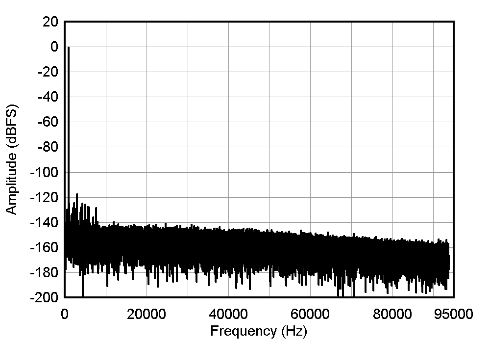
| G = 0.2 V/V, fIN = 1
kHz, SNR = 106.75 dB, THD = –115.95 dB |
Figure 9-10 Noise Performance FFT
Plots with Sinc4 Filter for G = 0.2 V/V
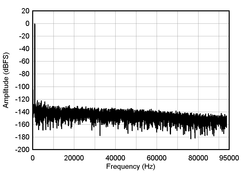
| G = 0.2 V/V, fIN = 1
kHz, SNR = 105.88 dB, THD = –122.00 dB |
Figure 9-11 Noise Performance FFT
Plots with Sinc4 Filter for G = 1 V/VTable 9-5 INA851 + ADS127L11 (Wideband
Filter) FFT Data Summary
| INPUT
AMPLITUDE (Vpk) |
RG RESISTOR
(Ω) |
GIN (V/V) |
GOUT
(V/V) |
SNR
(dB) |
THD
(dB) |
ENOB
(Bits) |
| 23.76015 |
None |
1 |
0.2 |
105.3 |
–116.2 |
17.14 |
| 4.7476 |
None |
1 |
1 |
103.1 |
–120.0 |
16.81 |
| 2.3738 |
1500 |
5 |
0.2 |
104.2 |
–113.0 |
16.85 |
| 0.2360 |
316 |
20 |
1 |
99.0 |
–112.0 |
16.08 |
| 0.0472 |
60.4 |
100 |
1 |
89.3 |
–99.0 |
14.40 |

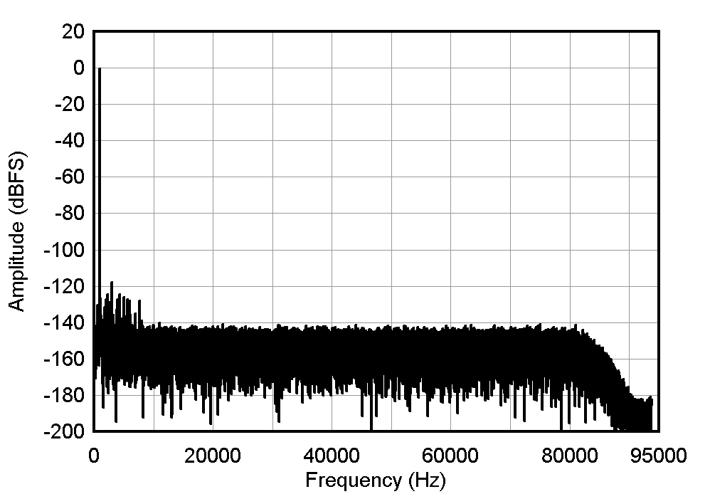
| G = 0.2 V/V, fIN = 1
kHz, SNR = 105.29 dB, THD = –116.21 dB |
Figure 9-12 Noise Performance FFT
Plots with Wideband Filter for G = 0.2 V/V
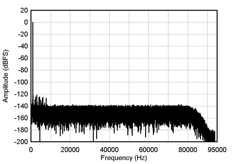
| G = 1 V/V, fIN = 1
kHz, SNR = 103.07 dB, THD = –120.01 dB |
Figure 9-13 Noise Performance FFT
Plots with Wideband Filter for G = 1 V/V
