ZHCSQ83A March   2022  – October 2022 INA851

PRODUCTION DATA  

  1. 特性
  2. 应用
  3. 说明
  4. Revision History
  5. Related Products
  6. Pin Configuration and Functions
  7. Specifications
    1. 7.1 Absolute Maximum Ratings
    2. 7.2 ESD Ratings
    3. 7.3 Recommended Operating Conditions
    4. 7.4 Thermal Information
    5. 7.5 Electrical Characteristics
    6. 7.6 Typical Characteristics
  8. Detailed Description
    1. 8.1 Overview
    2. 8.2 Functional Block Diagram
    3. 8.3 Feature Description
      1. 8.3.1 Adjustable Gain Setting
        1. 8.3.1.1 Gain Drift
      2. 8.3.2 Offset Voltage
      3. 8.3.3 Input Common-Mode Range
      4. 8.3.4 Input Protection
      5. 8.3.5 Output Clamping
      6. 8.3.6 Low Noise
    4. 8.4 Device Functional Modes
  9. Application and Implementation
    1. 9.1 Application Information
      1. 9.1.1 Output Common-Mode Pin
      2. 9.1.2 Output-Stage Gain Selection and Noise-Gain Shaping
      3. 9.1.3 Input Bias Current Return Path
      4. 9.1.4 Thermal Effects due to Power Dissipation
    2. 9.2 Typical Applications
      1. 9.2.1 Three-Pin Programmable Logic Controller (PLC)
        1. 9.2.1.1 Design Requirements
        2. 9.2.1.2 Detailed Design Procedure
        3. 9.2.1.3 应用曲线
      2. 9.2.2 20-Bit, 1-MSPS ADS8900B Driver Circuit With FDA Noise Filter
        1. 9.2.2.1 Design Requirements
        2. 9.2.2.2 Application Curves
      3. 9.2.3 24-Bit, 200 kSPS, Delta-Sigma ADS127L11 ADC Driver Circuit With FDA Noise Filter
        1. 9.2.3.1 Design Requirements
        2. 9.2.3.2 Application Curves
    3. 9.3 Power Supply Recommendations
    4. 9.4 Layout
      1. 9.4.1 Layout Guidelines
      2. 9.4.2 Layout Example
  10. 10Device and Documentation Support
    1. 10.1 Device Support
      1. 10.1.1 Development Support
        1. 10.1.1.1 PSpice® for TI
        2. 10.1.1.2 TINA-TI™ Simulation Software (Free Download)
    2. 10.2 Documentation Support
      1. 10.2.1 Related Documentation
    3. 10.3 接收文档更新通知
    4. 10.4 支持资源
    5. 10.5 Trademarks
    6. 10.6 Electrostatic Discharge Caution
    7. 10.7 术语表
  11. 11Mechanical, Packaging, and Orderable Information

封装选项

机械数据 (封装 | 引脚)
散热焊盘机械数据 (封装 | 引脚)
订购信息

Input Bias Current Return Path

The input impedance of the INA851 is very high at approximately 1 GΩ. However, a path must be provided for the input bias current of both inputs. This input bias current is typically 5 nA. High input impedance means that this input bias current changes very little with varying input voltage.

For proper operation, input circuitry must provide a path for input bias current. Figure 9-1 shows various provisions for an input bias current path. Without a bias current path, the inputs float to a potential that exceeds the common-mode range of the INA851, and the input amplifiers saturate. If the differential source resistance is low, the thermocouple example in Figure 9-1 shows that the bias current return path can connect to one input. With a higher source impedance, using two equal resistors provides a balanced input with the possible advantages of a lower input offset voltage as a result of bias current and better high-frequency common-mode rejection.

For more details about why a valid input bias current return path is necessary, see the Importance of Input Bias Current Return Paths in Instrumentation Amplifier Applications application report.
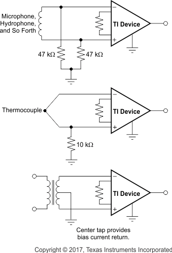
GUID-18588B4D-7DE9-4278-AC15-C38325483C82-low.gif Figure 9-1 Providing an Input Common-Mode Current Path