ZHCSIX1B October   2018  – December 2018 INA901-SP

PRODUCTION DATA.  

  1. 特性
  2. 应用
  3. 说明
    1.     Device Images
      1.      简化原理图
  4. 修订历史记录
  5. Pin Configuration and Functions
    1.     Pin Functions
  6. Specifications
    1. 6.1 Absolute Maximum Ratings
    2. 6.2 ESD Ratings
    3. 6.3 Recommended Operating Conditions
    4. 6.4 Thermal Information
    5. 6.5 Electrical Characteristics
    6. 6.6 Quality Conformance Inspection
    7. 6.7 Typical Characteristics
  7. Detailed Description
    1. 7.1 Overview
    2. 7.2 Functional Block Diagram
    3. 7.3 Feature Description
      1. 7.3.1 Basic Connection
      2. 7.3.2 Selecting RS
      3. 7.3.3 Transient Protection
    4. 7.4 Device Functional Modes
      1. 7.4.1 First- or Second-Order Filtering
      2. 7.4.2 Accuracy Variations as a Result of VSENSE and Common-Mode Voltage
        1. 7.4.2.1 Normal Case 1: VSENSE ≥ 20 mV, VCM ≥ VS
        2. 7.4.2.2 Normal Case 2: VSENSE ≥ 20 mV, VCM < VS
        3. 7.4.2.3 Low VSENSE Case 1: VSENSE < 20 mV, –16 V ≤ VCM < 0; and Low VSENSE Case 3: VSENSE < 20 mV, VS < VCM ≤ 80 V
        4. 7.4.2.4 Low VSENSE Case 2: VSENSE < 20 mV, 0 V ≤ VCM ≤ VS
  8. Application and Implementation
    1. 8.1 Application Information
    2. 8.2 Typical Application
      1. 8.2.1 Design Requirements
      2. 8.2.2 Detailed Design Procedure
      3. 8.2.3 Application Curves
  9. Power Supply Recommendations
  10. 10Layout
    1. 10.1 Layout Guidelines
      1. 10.1.1 RFI and EMI
    2. 10.2 Layout Example
  11. 11器件和文档支持
    1. 11.1 文档支持
      1. 11.1.1 相关文档
    2. 11.2 接收文档更新通知
    3. 11.3 社区资源
    4. 11.4 商标
    5. 11.5 静电放电警告
    6. 11.6 术语表
  12. 12机械、封装和可订购信息

封装选项

机械数据 (封装 | 引脚)
散热焊盘机械数据 (封装 | 引脚)
订购信息

Typical Characteristics

At TA = 25°C, VS = 12 V, VCM = 12 V, and VSENSE = 100 mV, unless otherwise noted.
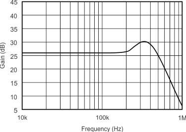
INA901-SP tc_g-frq_cl1k_bos938.gif
CLOAD = 1000 pF
Figure 1. Gain vs Frequency
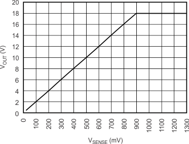
INA901-SP tc_gplot_bos938.gif
VS = 18 V
Figure 3. Gain Plot
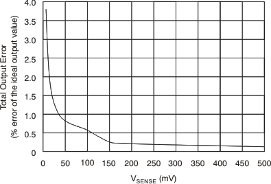
INA901-SP tc_err-vsense_bos381.gif
Figure 5. Total Output Error vs VSENSE
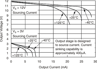
INA901-SP tc_pos_swing-io_bos381.gif
Figure 7. Positive Output Voltage Swing vs Output Current
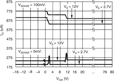
INA901-SP tc_iq-vcm_bos381.gif
Figure 9. Quiescent Current vs Common-Mode Voltage
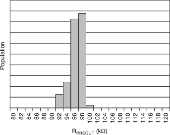
INA901-SP tc_histo_bos381.gif
Figure 11. PRE OUT Output Resistance Production Distribution
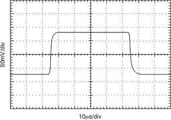
INA901-SP tc_step_sm_bos381.gif
Figure 13. Small-Signal Step Response
(10-mV to 20-mV Input)
INA901-SP tc_g-frq_cl0_bos938.gif
CLOAD = 1000 pF CLOAD = 0 pF
Figure 2. Gain vs Frequency
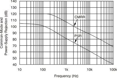
INA901-SP tc_cmrr_psrr-frq_bos381.gif
Figure 4. Common-Mode and Power-Supply Rejection vs Frequency
INA901-SP tc_err-vcm_bos381.gif
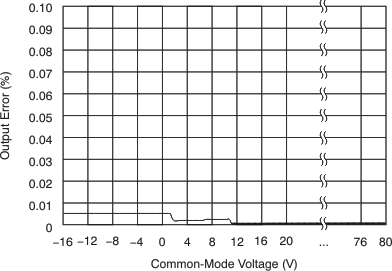
Figure 6. Output Error vs Common-Mode Voltage
INA901-SP tc_iq-vo_bos381.gif
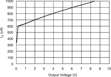
Figure 8. Quiescent Current vs Output Voltage
INA901-SP tc_cur-vs_bos381.gif
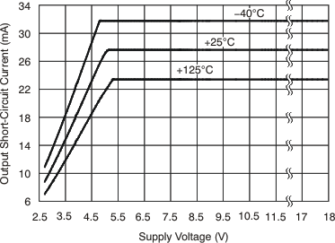
Figure 10. Output Short-Circuit Current vs Supply Voltage
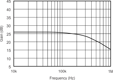
INA901-SP tc_buf_g-frq_bos381.gif
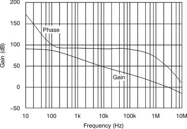
Figure 12. Buffer Gain vs Frequency
INA901-SP tc_step_lg_bos381.gif
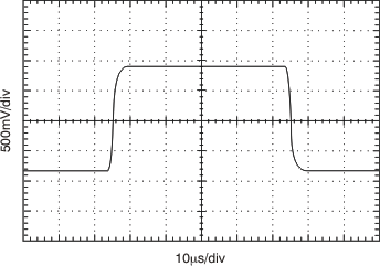
Figure 14. Large-Signal Step Response
(10-mV to 100-mV Input)