ZHCSA09F July 2012 – December 2022 ISO1540 , ISO1541
PRODUCTION DATA
- 1 特性
- 2 应用
- 3 说明
- 4 Revision History
- 5 Pin Configuration and Functions
-
6 Specifications
- 6.1 Absolute Maximum Ratings
- 6.2 ESD Ratings
- 6.3 Recommended Operating Conditions
- 6.4 Thermal Information
- 6.5 Power Ratings
- 6.6 Insulation Specifications
- 6.7 Safety-Related Certifications
- 6.8 Safety Limiting Values
- 6.9 Electrical Characteristics
- 6.10 Supply Current Characteristics
- 6.11 Timing Requirements
- 6.12 Switching Characteristics
- 6.13 Insulation Characteristics Curves
- 6.14 Typical Characteristics
- 7 Detailed Description
- 8 Application and Implementation
- 9 Power Supply Recommendations
- 10Layout
- 11Device and Documentation Support
- 12Mechanical, Packaging, and Orderable Information
5 Pin Configuration and Functions
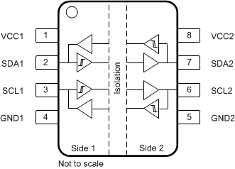
 Figure 5-1 ISO1540 D Package8-Pin SOICTop View
Table 5-1 Pin Functions—ISO1540
| PIN | I/O | DESCRIPTION | |
|---|---|---|---|
| NAME | NO. | ||
| GND1 | 4 | — | Ground, side 1 |
| GND2 | 5 | — | Ground, side 2 |
| SCL1 | 3 | I/O | Serial clock input / output, side 1 |
| SCL2 | 6 | I/O | Serial clock input / output, side 2 |
| SDA1 | 2 | I/O | Serial data input / output, side 1 |
| SDA2 | 7 | I/O | Serial data input / output, side 2 |
| VCC1 | 1 | — | Supply voltage, side 1 |
| VCC2 | 8 | — | Supply voltage, side 2 |
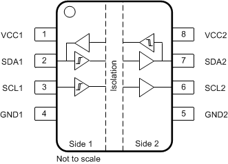
 Figure 5-2 ISO1541 D Package8-Pin SOICTop
View
Figure 5-2 ISO1541 D Package8-Pin SOICTop
ViewTable 5-2 Pin Functions—ISO1541
| PIN | I/O | DESCRIPTION | |
|---|---|---|---|
| NAME | NO. | ||
| GND1 | 4 | — | Ground, side 1 |
| GND2 | 5 | — | Ground, side 2 |
| SCL1 | 3 | I | Serial clock input, side 1 |
| SCL2 | 6 | O | Serial clock output, side 2 |
| SDA1 | 2 | I/O | Serial data input / output, side 1 |
| SDA2 | 7 | I/O | Serial data input / output, side 2 |
| VCC1 | 1 | — | Supply voltage, side 1 |
| VCC2 | 8 | — | Supply voltage, side 2 |